Chinese semiconductor industry

Status
Not open for further replies.

measuredingabens

Junior Member
Registered Member
This was the expected thing in the industry. A lot of my colleagues are kinda convinced that new nodes will appear every 3 years rather than 2 years going forward.

People I know at ASML were hopeful TSMC will use HiNA EUV for 2 nm. They likely won't.
Yeah, I've read news that Intel won't be using High NA for their 18A node either. It seems that low NA is still the way to go for the next few years. Though this does make me wonder about the kind of difficulty/cost in patterning 2nm with low NA vs high NA.
Please, Log in or Register to view URLs content!
 

56860

Senior Member
Registered Member
View attachment 119146View attachment 119147
Here is what huawei whisper is talking about Mate 5X vs iPhone side by side. You can see 5X camera captures light a lot better

View attachment 119148View attachment 119149
now iPhone and Mate 60 side by side. I will let you guess which one is Mate 60 and which one is iPhone

basically, i think people are going to see over time that Chinese suppliers can get you the best product and there is no need to use foreign chip/sensor suppliers. you don't need apple SoC, algo or Nikon camera to get the best photo qualities.
It may come as a shock to many, but being the world's factory for 40+ years means you get pretty good at making things.
 

tokenanalyst

Brigadier
Registered Member

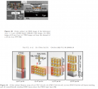
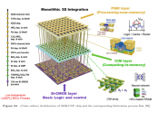
Recent progress in InGaZnO FETs for high-density 2T0C DRAM applications​


Shengzhe YAN1,2, Zhaori CONG1,2, Nianduan LU1 , Jinshan YUE1* & Qing LUO1 1 Institute of Microelectronics of the Chinese Academy of Sciences, Beijing 100029, China; 2University of Chinese Academy of Sciences, Beijing 100049, China Received 1 February 2023/Revised 29 March 2023/Accepted 9 June 2023/Published online 21 September 2023

Abstract:

In the past several decades, the density and performance of transistors in a single chip have been increasing based on Moore’s Law. However, the slowdown of feature size reduction and memory wall in the von Neumann architecture restrict the improvement of system performance and energy efficiency. Thus the requirements of the emerging big data and artificial intelligence applications cannot be met. To address this issue, novel devices and architectures are being explored. Among them, the InGaZnO (IGZO) fieldeffect transistor (FET) device and the computing-in-memory (CIM) architecture can be possible solutions for high-density, high-performance, and high-efficiency applications. Herein, we review the recent progress in IGZO-based FETs for dynamic random access memory (DRAM) applications. The mechanism of IGZO FETs, compact modeling of IGZO transistors, progress of IGZO manufacturing process, IGZO circuit design, and IGZO-based CIM and 3D integration architectures are presented. Furthermore, the challenges and future trends of IGZO research are discussed.​

1695411750839.png

1695411779586.png

Please, Log in or Register to view URLs content!
 

tphuang

Lieutenant General
Staff member
Super Moderator
VIP Professional
Registered Member

Recent progress in InGaZnO FETs for high-density 2T0C DRAM applications​


Shengzhe YAN1,2, Zhaori CONG1,2, Nianduan LU1 , Jinshan YUE1* & Qing LUO1 1 Institute of Microelectronics of the Chinese Academy of Sciences, Beijing 100029, China; 2University of Chinese Academy of Sciences, Beijing 100049, China Received 1 February 2023/Revised 29 March 2023/Accepted 9 June 2023/Published online 21 September 2023

Abstract:
In the past several decades, the density and performance of transistors in a single chip have been increasing based on Moore’s Law. However, the slowdown of feature size reduction and memory wall in the von Neumann architecture restrict the improvement of system performance and energy efficiency. Thus the requirements of the emerging big data and artificial intelligence applications cannot be met. To address this issue, novel devices and architectures are being explored. Among them, the InGaZnO (IGZO) fieldeffect transistor (FET) device and the computing-in-memory (CIM) architecture can be possible solutions for high-density, high-performance, and high-efficiency applications. Herein, we review the recent progress in IGZO-based FETs for dynamic random access memory (DRAM) applications. The mechanism of IGZO FETs, compact modeling of IGZO transistors, progress of IGZO manufacturing process, IGZO circuit design, and IGZO-based CIM and 3D integration architectures are presented. Furthermore, the challenges and future trends of IGZO research are discussed.​

View attachment 119152

View attachment 119153

Please, Log in or Register to view URLs content!

I think Huawei issued that study/report last year right?

Please, Log in or Register to view URLs content!

it will be interesting to see how long it would take them to put this into practice with Swaysure.

Also, I wonder how far along CXMT is with its own effort here.
 

latenlazy

Brigadier
This was the expected thing in the industry. A lot of my colleagues are kinda convinced that new nodes will appear every 3 years rather than 2 years going forward.

People I know at ASML were hopeful TSMC will use HiNA EUV for 2 nm. They likely won't.
Technically 3 nm took 3 years and if you count the fact that only Apple has access to it for everyone else it’s more like 4 year. Judging by the results from the A17 TSMC’s N3B fell short of expectations in performance gain too. Wouldn’t be surprised if 2 nm gets pushed back even further than 2026 as they try to develop it.
 

latenlazy

Brigadier
I think Huawei issued that study/report last year right?

Please, Log in or Register to view URLs content!

it will be interesting to see how long it would take them to put this into practice with Swaysure.

Also, I wonder how far along CXMT is with its own effort here.
I need to look into the details later but I think this IGZO transistor proposal is different from the vertical transistor Huawei proposed.
 

tokenanalyst

Brigadier
Registered Member
This work is probably related but by different institutions.

Cell Structure and Process Integration of a Novel 2T0C Technology for High-Density Dram Application​

Beijing Superstring Academy of Memory Technology, Beijing, China
Key Laboratory of Microelectronics Devices and Integrated Technology, Institute of Microelectronics, Chinese Academy of Sciences, Beijing, China


Abstract:
A new DRAM 2T0C cell is introduced to resolve those special issues for traditional 2T0C DRAM. In this technology, the read transistor holds dual gates. The data is stored in one gate of read transistor, and the other gate is used to control read operation. By writing different-level voltages into storage gate, the read transistor will have different threshold voltages by using the other gate as control gate. Compared with 1T1C DRAM, read operation in this new technology is non-destructive and therefore no explicit capacitor is required. Low leakage is essential for write transistor to obtain long data retention time. A few cell structures of this new 2T0C technology are discussed for high-density DRAM application, and challenges of process integration is also analyzed.​


Please, Log in or Register to view URLs content!
 

siegecrossbow

General
Staff member
Super Moderator
View attachment 119146View attachment 119147
Here is what huawei whisper is talking about Mate 5X vs iPhone side by side. You can see 5X camera captures light a lot better

View attachment 119148View attachment 119149
now iPhone and Mate 60 side by side. I will let you guess which one is Mate 60 and which one is iPhone

basically, i think people are going to see over time that Chinese suppliers can get you the best product and there is no need to use foreign chip/sensor suppliers. you don't need apple SoC, algo or Nikon camera to get the best photo qualities.

Is the difference purely because of camera hardware or does software also play an integral part? I find it hard to believe that Apple would skimp out on iPhone cameras.
 

tphuang

Lieutenant General
Staff member
Super Moderator
VIP Professional
Registered Member
Is the difference purely because of camera hardware or does software also play an integral part? I find it hard to believe that Apple would skimp out on iPhone cameras.
There is the camera sensors itself with the lens sensors, optical module (their drivers & software for that). There is also the SoC itself with its ISP & NPU which does the hard work of translating that data into photos

I need to look into the details later but I think this IGZO transistor proposal is different from the vertical transistor Huawei proposed.
I need to do so too. Seems like this is the direction Chinese DRAM makers have to go down before EUV is available
 
Status
Not open for further replies.
Top