Chinese semiconductor industry

Status
Not open for further replies.

taxiya

Brigadier
Registered Member
so i heard apparently CIOMP is not great institution

I looked back on all the images i collected on EUVs

I see at least 4 patents from SIOM and nothing from CIOMP

The only thing i see from CIOMP is that CAS visit.

@tokenanalyst do you know what I mean?

something fishy about SIOM in so many patents, but CIOMP building prototype?
CIOMP specializes in optics and machenics, like telescope lenses and satellite camera including the stablizer structures. We know all those optical observation sats are from CIOMP. SIOM started in 1964 focusing on laser as its website says. So they have different areas of expertise.

For EUV, I can see the job natually divided between the two. SIOM works on the light source, CIOMP build the machine.
 

jfcarli

Junior Member
Registered Member
I don't blame you, the headlines make it seem like there's only 1 true correct path, but that's all post-hoc justification.

What exactly is economical about using a 100 kW CO2 laser that weighs 10000+ kgs alone to shoot liquid tin droplets in vacuum that's in another 10+ ton system? liquids and vacuum doesn't mix well, exploding metallic liquids even less so, so you need a very sophisticated metal management system to handle the outgassing and cleanup of lenses. And that's not even getting to the optics transmission train, wafer stage, etc.

Just a single EUV instrument can buy the entire Shanghai Synchrotron.

Please, Log in or Register to view URLs content!


The difference is the Shanghai Synchrotron has 16 beamlines, not 1, and are energy tunable.

Please, Log in or Register to view URLs content!

Please, Log in or Register to view URLs content!


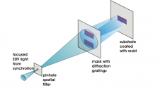
Note that they're using EUV interference lithography here. Interference lithography is maskless. Wave interference is only meaningful with coherent light. Regular EUV is not a laser. It uses a laser as the energy source for Sn droplet excitation, but the EUV itself, emitted by the Sn droplets, is isotropic.

Synchrotrons produce coherent EUV, which opens up tons of possibilities that don't exist with incoherent LPP EUV. It's not a mere economic advantage (more beamlines for the price of 1), it's a technical one.

And this is not even a synchrotron optimized for EUV production, it just happens to have this capability at 1 beamline station.
"The difference is the Shanghai Synchrotron has 16 beamlines, not 1, and are energy tunable."

I wonder if you could clarify whether those 16 beamlines could each of them feed one separate litography assembly line. If yes, and one could spread the cost among 16 different equipments, an equivalent to the Shangai Synchrotron would cost a "mere" US 10 million per litography machine.

If this is the case, I see no point whatsoever in pursuing to reproduce the lighting source used by ASML. That lighting source only makes sense if you have to transport the whole ensemble across the ocean.

As you say "What exactly is economical about using a 100 kW CO2 laser that weighs 10000+ kgs alone to shoot liquid tin droplets in vacuum that's in another 10+ ton system?"

Using a synchrotron source you could build the whole assembly lines as appendixes adjacent to the synchrotron itself, since no one will have to move the equipment anywhere else.

I wonder if you would need reflecting mirrors or just plain lenses to imprint the wafers. The picture below seems to say no mirrors, but obviously this is a gross over simplification.

If no mirrors are needed, there is no need for Zeiss optics.


1695329142017.png1695329142017.png
 

latenlazy

Brigadier
"The difference is the Shanghai Synchrotron has 16 beamlines, not 1, and are energy tunable."

I wonder if you could clarify whether those 16 beamlines could each of them feed one separate litography assembly line. If yes, and one could spread the cost among 16 different equipments, an equivalent to the Shangai Synchrotron would cost a "mere" US 10 million per litography machine.

If this is the case, I see no point whatsoever in pursuing to reproduce the lighting source used by ASML. That lighting source only makes sense if you have to transport the whole ensemble across the ocean.

As you say "What exactly is economical about using a 100 kW CO2 laser that weighs 10000+ kgs alone to shoot liquid tin droplets in vacuum that's in another 10+ ton system?"

Using a synchrotron source you could build the whole assembly lines as appendixes adjacent to the synchrotron itself, since no one will have to move the equipment anywhere else.

I wonder if you would need reflecting mirrors or just plain lenses to imprint the wafers. The picture below seems to say no mirrors, but obviously this is a gross over simplification.

If no mirrors are needed, there is no need for Zeiss optics.


View attachment 119116View attachment 119116
Each beam line needs to have adequate light output first, and if the synchrotron is too big it will have negative downstream impacts on the rest of your workflow logistics, since you still need to move wafers back and forth between scanning steps.
 

jfcarli

Junior Member
Registered Member
Each beam line needs to have adequate light output first, and if the synchrotron is too big it will have negative downstream impacts on the rest of your workflow logistics, since you still need to move wafers back and forth between scanning steps.

Each beam line needs to have adequate light output first, and if the synchrotron is too big it will have negative downstream impacts on the rest of your workflow logistics, since you still need to move wafers back and forth between scanning steps.
Makes sense. Didn't think of the industrial process. Any thougts as to how to still use the sychrotron, despite its size?
 

tokenanalyst

Brigadier
Registered Member

Institute of Microelectronics has made new progress in research in the field of low-power artificial intelligence​

Recently, the low-power intelligent technology and microsystem team of the Institute of Microelectronics’ Perception Center has made new progress in the field of low-power artificial intelligence.
  Voice wake-up technology ( KWS, Keyword Spotting ) is an important technology in the field of artificial intelligence. As an audio "switch" for devices and systems, it is widely used in various low-power smart chips and microsystems. In existing research on low-power voice wake-up chips, there is still a problem of mismatch between voice features and network model accuracy, which hinders further reduction of chip power consumption.
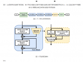
  In response to the above problems, the scientific research team of the Perception Center proposed an extremely lightweight, high-accuracy binary voice wake-up system, which consists of a voice feature binarization method based on error diffusion ( Error-Diffusion , Figure 1 ) and a binary voice wake-up system. It is composed of convolutional neural network TC-BiReal8 (Figure 2 ). By quantizing speech features, network activation values, and network weight values into 1 bit ( +1 , -1 ), this system not only significantly reduces memory usage, but also eliminates all high-bit-width multiplication operations required in traditional speech wake-up neural networks. , extremely friendly to extremely low-power hardware implementation. In order to solve the problem of accuracy decrease caused by the binary network, the team proposed an improved shortcut module (Figure 3) in the TC-BiReal8 network , which enhanced the residual path in the binary convolution module. Representation ability. Under the single-keyword and double-keyword recognition tasks of the GSCD (Google Speech Commands Dataset) v1 standard speech data set, the wake-up accuracy of the system is 98.54% and 95.05% respectively, which is twice the 8-bit DSCNN-m speech stored in the system. wake-up system, respectively higher than 0.3% and1.98% , and it is estimated that more than 17 times of normalized energy consumption savings can be achieved , laying a good foundation for the subsequent low-power hardware implementation of the system.


1695341342398.png

Please, Log in or Register to view URLs content!
 

tokenanalyst

Brigadier
Registered Member

Tuojing Technology: PE-ALD equipment has achieved mass production, and SACVD and HDPCVD equipment have achieved industrialization​

recently accepted an institutional survey and stated that the ALD equipment series developed by the company include PE-ALD equipment and Thermal-ALD equipment. The PE-ALD equipment has achieved mass production and can deposit SiO2, SiN and other dielectric film materials, Thermal-ALD equipment has been shipped to different clients for verification, and can deposit Al2O3 and other metal compound films; SACVD and HDPCVD equipment have been industrialized. The company will continue to maintain the core competitive advantages of its products and continue to expand the scale of mass production applications.

Please, Log in or Register to view URLs content!
 

interestedseal

Junior Member
Registered Member
I found the original link

Please, Log in or Register to view URLs content!

Question: Dr. Zhu Yu, is there any gap between the workpiece table developed by your research group and ASML company, or what gaps still exist?
Answer: At present, the workpiece table developed by our research group is at the same level as the most advanced workpiece table (products above 2000 series) of ASML company in a large generation. However, there is still a generation gap with ASML's 2000 series and above products in a small generation, and it can catch up with the international advanced level after one more iteration.

View attachment 117482


Please, Log in or Register to view URLs content!

Professor Zhu Yu is the founder of Uprecision and Hwatsing
In other news, premier Li Qiang visited Uprecision today. What do you guys make of this visit? Any significance?
Please, Log in or Register to view URLs content!
 

ansy1968

Brigadier
Registered Member
In other news, premier Li Qiang visited Uprecision today. What do you guys make of this visit? Any significance?
Please, Log in or Register to view URLs content!
UPrecision had finished its expansion plan and is already mass producing its Dual Stage equipment. We may hear an official unveiling of the SSA800 28NM Duvi soon after the US announce a new set of sanction. ;)
 
Status
Not open for further replies.
Top