Chinese semiconductor industry

Status
Not open for further replies.

tokenanalyst

Brigadier
Registered Member

Domestic semiconductor measurement equipment manufacturer Fabosi completed tens of millions of yuan in Series A financing​


Farbus (Ningbo) Semiconductor Equipment Co., Ltd. (hereinafter referred to as "Fabables") has recently completed tens of millions of yuan in Series A financing, led by Hefei Dunqin, And Xingniu Capital, founded by executives such as Intel and ARM, jointly invested. The funds raised in this round will be mainly used for R&D team expansion, marketing promotion, DEMO machine production and new product development, etc.
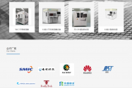
Founded in 2019, Fabos is a semiconductor measurement equipment developer, committed to providing localized, independent and controllable measurement equipment for customers in the semiconductor industry. The customer groups that have shipped include SMIC, JCET, ASE, etc. .
The Fabos team has a size of more than 20 people, and R&D personnel account for about 80%. Among them, the core members are mainly from world-renowned enterprises and institutions such as Sharp China R&D Center, Tianjin University, and Shanghai Jiaotong University. Founder and CEO Song Jinlong once worked for Sharp and Lenovo Research Institute, and has been deeply involved in 3D algorithms, visual inspection and measurement; COO Zhu Jianguo has rich experience in the semiconductor industry, and has successively worked for Haier Integrated Circuits, Belling shares, British Plessy and other semiconductor companies.
In terms of product lines, the company's current core products include two categories: substrate inspection equipment, and wafer-level advanced packaging inspection equipment. Among them, the substrate inspection equipment includes various substrate geometries and defects including large silicon wafers and three and a half generations; wafer-level advanced packaging inspection equipment includes 2D/3D defect inspection, roughness, TSV and other contour inspection and OVERLAY and CD detection.
1693794220009.png
Please, Log in or Register to view URLs content!
 

tphuang

Lieutenant General
Staff member
Super Moderator
VIP Professional
Registered Member
looks like this one thinks PPA is between 118 & 121, which would put it as the same level as N7+, better than what Intel has done & better than Samsung 5LPE. Depending on how this is measured, could be better than N7+.

@Alb's chart of SMIC roadmap may be true after all
Screen Shot 2023-09-03 at 10.46.10 PM.png

N+1 is basically a borderline 7nm
N+2 is somewhere bw late 7nm & early 5nm if this is the case

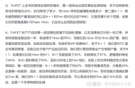
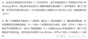
From 2020
18a5abeb09542b43fe550cdf.png!custom.jpg.png
18a5abe7f2c236a23fc14bcb.png!custom.jpg.png
At the time, analysts of SMIC noted that SMIC's N+1 was very close to TSMC 7nm performance based on the question from 1st picture. They also said that N+2 is next step. Cost similar and N2 will not use EUV. But N+2 will obviously be significantly improved.

So if October sanction didn't come, I think it's reasonable to expect SMIC to get to bw TSMC N5 & Samsung 4LPE with N+3 or N+2 improved by Kirin 9100.

With October sanctions, they may have to be content on just further improving yield on N+2 process.

I don't know if Kirin 9100 will be supported by a noticeably higher density process. so any improvement will have to come from improved Taishan core, Maleon GPU, modem, NPU/TPU & larger die space (or advanced packaging/stacking)
 

ansy1968

Brigadier
Registered Member
The article "Research on 100 kHz Repetition Frequency Tin Droplet Target" submitted by the institute's team introduces the team's research progress on the tin droplet generator, a core component of the laser plasma extreme ultraviolet (LPP-EUV) lithography light source.

Please, Log in or Register to view URLs content!
Sir regarding your Twitt about Qingdao FAB, is this the one Huawei bought from SMIC?
 

olalavn

Senior Member
Registered Member
Raimondo: we will dump prices chips... =))

U.S. Commerce Secretary Raimondo said on September 3 that the economic relationship between China and the United States is mutually beneficial, and open communication channels are the key to maintaining this relationship. In the field of semiconductors, Raimondo said that the United States will continue to export chips to China, but we won't sell the most advanced and powerful chips to China.

Please, Log in or Register to view URLs content!
 

azn_cyniq

Junior Member
Registered Member
looks like this one thinks PPA is between 118 & 121, which would put it as the same level as N7+, better than what Intel has done & better than Samsung 5LPE. Depending on how this is measured, could be better than N7+.

@Alb's chart of SMIC roadmap may be true after all
View attachment 118151

N+1 is basically a borderline 7nm
N+2 is somewhere bw late 7nm & early 5nm if this is the case

From 2020
View attachment 118149
View attachment 118150
At the time, analysts of SMIC noted that SMIC's N+1 was very close to TSMC 7nm performance based on the question from 1st picture. They also said that N+2 is next step. Cost similar and N2 will not use EUV. But N+2 will obviously be significantly improved.

So if October sanction didn't come, I think it's reasonable to expect SMIC to get to bw TSMC N5 & Samsung 4LPE with N+3 or N+2 improved by Kirin 9100.

With October sanctions, they may have to be content on just further improving yield on N+2 process.

I don't know if Kirin 9100 will be supported by a noticeably higher density process. so any improvement will have to come from improved Taishan core, Maleon GPU, modem, NPU/TPU & larger die space (or advanced packaging/stacking)
I apologize if this has been mentioned before, but do we know if SMIC's N+2 process uses indigenous lithography systems?
 
Status
Not open for further replies.
Top