Chinese semiconductor industry

Status
Not open for further replies.

tphuang

Lieutenant General
Staff member
Super Moderator
VIP Professional
Registered Member
Well, SMEE hadn't announced their SA800 yet. So the way I see it, the upcoming announcement could be about that. And the implication is that the SA800 is already producing the Kirin 9000s. It only really said there's more to come after the 9000s and to get ready for surprises.

The SA800 may not surprise any of us, because we'll we've been following this like flies on honey. But I think most of the world would be shocked by a 28nm DUVi.
Ssa800 was not involved in making of Kirin 9000s based on all the legit industry insiders that have commented on this forum and on zhihu

This is insanely speculative of my part but if Huawei and SMIC are patterning finfet transistors using EUV Free Electron Lasers or SSMB that would the bombshell of the century, it will flip the entire semiconductor industry.
Let's wait for Kirin 9100 to determine.

If first Kirin 9000s was tested out at end of 2020, that's way too early of timeline for this. Even if good chunk of the chips were fabbed in 2022, euv wouldn't really work from timeline point of view


As for surprises, have people considered that Kirin a2 on 14nm process coming out would be another nice surprise? there are more also.they make plenty of progress without euvs
 

tonyget

Senior Member
Registered Member
"our self-developed lithography machine"?!?!?! "They have all worked tirelessly for three years."?!?!?! "Harbin Institute of Technology, Changchun Institute of Optics and Mechanics, etc.."?!?!?!

Ok, now we are officially in fiction territory, Hollywood should take note.

Not that I don't believe it (we will see), what I say is that this is really panning out like a movie drama, something that if it was scripted by a Hollywood writer, it would have been discarded because not enuogh credible....

In original Chinese context,the word "our" refer to China not Huawei
 

tphuang

Lieutenant General
Staff member
Super Moderator
VIP Professional
Registered Member
I re-watched the youtube clip over 9000S. A lot of interesting stuff there

The presence of NPU is something I haven't thought about before Including mini Ascend Tini/Lite & Da Vinci NPU. Not sure how it compares to the NPU on Snapdragon 8 Gen 2. But considering Hisilicon's experience in this area, I would think it should be very competitive here.

The power consumption on 9000S was better than I thought. For example, power consumption on 4-core A510 at low frequency was slightly better than that of Samsung 4LPE (first gen 4nm).

The 3 medium core Taishan at 1.9GHz was comparable (slightly worse) in performance & power consumption to Cortex A710 (on Snapdragon 8 Gen 1) fabbed on Samsung 4LPE. Again, unexpected

Only the large core Taishan at 2.6GHz was a little worse than Arm Cortex X1 (Snapdragon 888) in performance & a lot worse in power consumption. It was even more inferior to Arm Cortex X2 (Snapdragon 8 Gen 1)

Overall, it's extreme performance had higher score than all except Snapdragon 8 Gen 2 (including Gen 1 & Kirin 9000)
power consumption/performance was better than Snapdragon 888, but worse than Snapdragon 8 Gen 1

The reviewer concluded that more work needs to be done with hyper threading on CPU (which is inherited from Kunpeng design)

imo, the higher power consumption is expected

Hisilicon is designing its own CPU core + GPU here. You can't blame some of the under performance on power consumption to SMIC process. Seems like it's just as Hisilicon related. But thankfully, power consumption can be overcome by better battery tech + heat dissipation. They have both. Peak performance seems plenty enough. And as they adjust more to high end games, it should work even better.
 

siegecrossbow

General
Staff member
Super Moderator
I re-watched the youtube clip over 9000S. A lot of interesting stuff there

The presence of NPU is something I haven't thought about before Including mini Ascend Tini/Lite & Da Vinci NPU. Not sure how it compares to the NPU on Snapdragon 8 Gen 2. But considering Hisilicon's experience in this area, I would think it should be very competitive here.

The power consumption on 9000S was better than I thought. For example, power consumption on 4-core A510 at low frequency was slightly better than that of Samsung 4LPE (first gen 4nm).

The 3 medium core Taishan at 1.9GHz was comparable (slightly worse) in performance & power consumption to Cortex A710 (on Snapdragon 8 Gen 1) fabbed on Samsung 4LPE. Again, unexpected

Only the large core Taishan at 2.6GHz was a little worse than Arm Cortex X1 (Snapdragon 888) in performance & a lot worse in power consumption. It was even more inferior to Arm Cortex X2 (Snapdragon 8 Gen 1)

Overall, it's extreme performance had higher score than all except Snapdragon 8 Gen 2 (including Gen 1 & Kirin 9000)
power consumption/performance was better than Snapdragon 888, but worse than Snapdragon 8 Gen 1

The reviewer concluded that more work needs to be done with hyper threading on CPU (which is inherited from Kunpeng design)

imo, the higher power consumption is expected

Hisilicon is designing its own CPU core + GPU here. You can't blame some of the under performance on power consumption to SMIC process. Seems like it's just as Hisilicon related. But thankfully, power consumption can be overcome by better battery tech + heat dissipation. They have both. Peak performance seems plenty enough. And as they adjust more to high end games, it should work even better.

Are there video game performance benchmark videos out on popular games like PUBG and Genshin?
 

tphuang

Lieutenant General
Staff member
Super Moderator
VIP Professional
Registered Member
Are there video game performance benchmark videos out on popular games like PUBG and Genshin?
No idea. I don't want to judge them too harsh now because it's a new GPU for video games and it might take sometimes for them to sort out compatibility issues with various games. I do have hope now that Huawei will design it's own notepad GPU and then desktop GPU.

It's worth noting the importance of designing your own cpu and GPU. During game play, the two showed very compatible cpu & GPU usage. So neither was overworked


Also, the process used is quite mysterious

This chip was not stacked. Its surface area was 110 mm2, just slightly greater than Kirin 9000 but had better overall performance, although with worse energy consumption. I would have expected it to be larger to squeeze in more transistors or stacked.

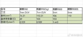
In terms of transistor density, the infamous 7nm n+1 chip had density of 91 million transistors per mm2.

In Kirin 980 & 990, both had around 90 to 93 million per mm2. So n+1 was already as dense as earliest N7.

Kirin 9000 had density of 144 million per mm2 using n5 process. It's hard for me to see this n+2 process not having at least 110 million per mm2. I wouldn't be surprised if it's as high as 120 million per mm2. Which would be equivalent to Samsung 5nm process. Longer term, I think 140 million per mm2 is possible
 

ansy1968

Brigadier
Registered Member
Well, we all followed and are following the SMEE saga since the past 3 years. Like almost anybody in this forum, our view is/was that all DUVi and bigger node lithography was on SMEE shoulders....regarding EUV we know there are different actors developing it, but DUV was/is a SMEE thing.
Don't forget CETC, they're able to develop a satellite chip by using domestic tools since they are under sanction for years. I think working with Huawei they're able to make it commercially viable.
 

supercat

Major
CETC.

Please, Log in or Register to view URLs content!

Please, Log in or Register to view URLs content!

Please, Log in or Register to view URLs content!

Please, Log in or Register to view URLs content!


Please, Log in or Register to view URLs content!

Sep 6, 2022 — TAIPEI -- Huawei Technologies has included satellite ... said Huawei used a chip from developer CETC Acoustic-Optic-Electronic Technology to ...
Here is the article without paywall:
Please, Log in or Register to view URLs content!

Both China's 5G network and the Huawei Mate 60 Pro are amazing.
 

tphuang

Lieutenant General
Staff member
Super Moderator
VIP Professional
Registered Member
I'm now getting super curious of this TechInsight report, because

1) here is the Transistor analysis from various Apple SoC
AppleSoc_TransistorComparison.png
Notice the obvious jump in transistor density from N7 to N5 and transistor count
Why is Apple A14 Bionic better than Apple A13 Bionic?
  • 7.2% faster CPU speed. ...
  • 2nm smaller semiconductor size. ...
  • 450MHz faster GPU clock speed. ...
  • Uses HMP.
  • Has 5G support.
  • 19.16% higher single-core Geekbench 5 result. ...
  • 29.02% higher multi-core Geekbench 5 result. ...
  • 3300million more transistors

2) now Kirin 9000 vs Kirin 980/990
KirinSocs_TransistorComparison.jpg
Again, not the huge jump in transistor desnity from 90m to 144m when going from N7 to N5

This is what we know.
9000S CPU performance better than 9000
It has a full 5G built in modem like 9000
barely any increase in die size
has 1/4 of die dedicated to GPU with 4 computing units
Separate NPU with Da Vinci NPU, Ascend lite/mini cores & Tensor unit that is separate from DPU
all of this built in to same space as Kirin 9000 without any chip stacking

When N+1 came out, tech insight reported 91million transistors/mm2, similar to Kirin 980/990

So unless there ia somehow a dramatic decrease in transistor count (which seems unlikely given all the features)

imo, we are looking at a N7+ process or even close to N5.

But let's wait and see. All of this is surprising

Think about this
Please, Log in or Register to view URLs content!
Qualcomm Snapdragon (look at slide 16) does not have its own separate NPU from what I can see

Please, Log in or Register to view URLs content!
samsung Exynos looks like it has a joint NPU/DSP area. Doesn't look as large as Kirin 9000s

Iphone A15 looks more comparable to Kirin 9000s in NPU size.
Seems like Kirin 9000s should have advanced Machine learning for a phone SoC
 
Last edited:

tonyget

Senior Member
Registered Member
I'm now getting super curious of this TechInsight report, because

1) here is the Transistor analysis from various Apple SoC
View attachment 118142
Notice the obvious jump in transistor density from N7 to N5 and transistor count


2) now Kirin 9000 vs Kirin 980/990
View attachment 118144
Again, not the huge jump in transistor desnity from 90m to 144m when going from N7 to N5

This is what we know.
9000S CPU performance better than 9000
It has a full 5G built in modem like 9000
barely any increase in die size
has 1/4 of die dedicated to GPU with 4 computing units
Separate NPU with Da Vinci NPU, Ascend lite/mini cores & Tensor unit that is separate from DPU
all of this built in to same space as Kirin 9000 without any chip stacking

When N+1 came out, tech insight reported 91million transistors/mm2, similar to Kirin 980/990

So unless there ia somehow a dramatic decrease in transistor count (which seems unlikely given all the features)

imo, we are looking at a N7+ process or even close to N5.

But let's wait and see. All of this is surprising

Think about this
Please, Log in or Register to view URLs content!
Qualcomm Snapdragon (look at slide 16) does not have its own separate NPU from what I can see

Please, Log in or Register to view URLs content!
samsung Exynos looks like it has a joint NPU/DSP area. Doesn't look as large as Kirin 9000s

Iphone A15 looks more comparable to Kirin 9000s in NPU size.
Seems like Kirin 9000s should have advanced Machine learning for a phone SoC

I think they can tell which fab made the chip,or unidentified fab in case it's Huawei's own fab. Because each fab's process is patented,so they must have different structure.
 
Status
Not open for further replies.
Top