Chinese semiconductor industry

Status
Not open for further replies.

tphuang

Lieutenant General
Staff member
Super Moderator
VIP Professional
Registered Member
Capture.JPG
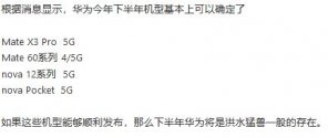
This is quite a lot of 5G phones announced for rest of the year. From the Huawei Whisper, who is normally quite accurate on these things.
The announcement for Mate 60 and Mate X3 Pro 5G expected so happen in a month based on these social media posting.

That tells me they got the 5G supply chain up and producing already
 

tokenanalyst

Brigadier
Registered Member

Keystone signed a new customer order for 12-inch wafer fab.​

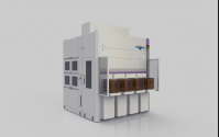
Shanghai Keystone Semiconductor Co., Ltd. (hereinafter referred to as "Keystone") recently signed a sales order for a 12-inch ion implanter with a new customer of a logic chip fab.

As a leader in the industrialization of domestically produced low-energy, large-beam and high-energy ion implanters, Kaistone has signed purchase orders with a number of mainstream customers of 12-inch integrated circuit manufacturing plants since 2020, with a cumulative amount of over 1 billion yuan.

In the future, Keystone will practice the concept of CIP continuous improvement, continue to expand the upper limit of technology, continue to improve industrialization capabilities, and help customers increase mass production.

Please, Log in or Register to view URLs content!
 

tphuang

Lieutenant General
Staff member
Super Moderator
VIP Professional
Registered Member
My notes from SMIC earnings call. Took me a long time to listen through this because I had to stop the playback multiple times to make sure I get the gist down. I think China's Semiconductor industry is lucky to have SMIC, because it is really tasked with a lot of responsibility. Many times, they stated that they have 10 platforms at each node in order to capture all the products and demands. Which makes sense given the need to have everything built locally. Anyhow, the good news is that both Jingcheng & Shenzhen have started mass production & SMIC is quickly building up volume to a breakeven point right now, especially with a lot of 28/40/55nm capacity

Lingang is building production line too and Tianjin is getting roofed now. Everything is coming together. Just needs more time. Demand for SMIC services in more advanced nodes (and even nodes that many westerners don't consider advanced like 55/65nm) are very high. This is not a problem that foreign fabs have to "deal with". SMIC really needs to ramp up quickly so that TSMC & UMC don't come in with their additional 28nm capacity and take everything


Now I need to listen to Huahong's earnings call. another long one!

I think anyone that thinks of themselves as a semi industry expert and don't listen to SMIC earnings call are just kidding themselves.

While we often talk about reaching the limit of shrinking transistors for your advanced process, many other process already got there.

For example, SMIC started at 38nm in NAND flash 9 years ago and then was able to produce 24nm NAND a few years after that. IIRC, state of the art is like 19nm? but seems like customers are not asking SMIC to go below 24nm, so they are basically at the end point there

With NOR flash, it announced that it was able to do 40nm at earnings call, It was already able 40nm embedded flash 3 years ago. When Gigadevice came out with its 40nm low power embedded flash, it had to be fabbed at TSMC
Please, Log in or Register to view URLs content!

Now, all of this can be fabbed at SMIC. Given the de-risking pressures, it will be very motivated to validate SMIC for same chip. SMIC just needs to make sure its chips are auto grade.

For a lot of these chips, it seems like 28nm and 40nm process is the end point. You are not getting much performance gain beyond that.

SMIC itself mentioned BCD, LCD driver & MCUs as processes that once you get to 40/28nm, there is probably no reason to go beyond that. As such, while SMIC still has work to do in making sure its 28nm product line covers all the platforms, we are probably just a couple of quarters from that. By this point next year, I will be very annoyed if SMIC doesn't have full product line at these nodes to compete against TSMC & UMC in its own backyard. It should be adding at least 40k 12-inch wpm of 28/40nm process by then. SMIC itself even mentions that 10k wpm is not enough to break even, so Jingcheng & Shenzhen both probably need to add at least 20k wpm.

Its fully booked for 55nm and above. There is clearly demand for them to rapidly add more. And the more they add and more specialty platforms they can add, the more domestic supply chain can de-risk and capture larger market share. During this time, Chinese govt can help them by slowing down the approval process for TSMC & UMC expansion. Longer term, I have no issue with TSMC/UMC expanding here. Looking at how many chips China still imports, they need more fabs to produce in China. But in shorter term, delaying those two's expansion gives SMIC a chance to really expand and be on the right path to be world's #2 behind TSMC.
 
Last edited:

olalavn

Senior Member
Registered Member
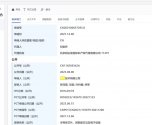
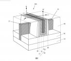
Huawei's Semiconductor chip, its manufacturing method and electronic device

Screenshot 2023-08-13 230834.png

The application discloses a semiconductor chip, its preparation method and electronic equipment. Wherein, the semiconductor chip includes a substrate and a Fin FET located on the substrate; the FinFET includes: a fin, two side walls opposite to each other across the fin, and a gate located in a trench defined by the two side walls. electrode structure; the gate structure includes a gate dielectric layer and a bar metal layer arranged in sequence, and the gate metal layer includes a TISIN layer, that is, the TISIN material is used to fill the void. In the process of filling the TISIN, due to the Si doping can be The lattice structure of TIN is destroyed, so that the formed TISIN thin film becomes an amorphous film, and the voids will not be sealed in advance due to excessive crystal grains. Therefore, the TISIN layer in the gate structure provided by this application has excellent gap filling ability. It can achieve high aspect ratio without filling, and TiSiN with low silicon concentration has a resistivity similar to or even lower than TIN, so a gate structure with low resistivity can be realized.Screenshot 2023-08-13 230834.pngd253a4259b5b37619da9351619097fb9487936744.png.jpge4868daa1261042c5db0e130c6724d50487936744.png@!web-comment-note.jpg
 
Last edited:

olalavn

Senior Member
Registered Member
Creating a new path for quantum state control and transmission, Xiamen University successfully developed a topological spin solid-state light source chip

Please, Log in or Register to view URLs content!

Anhui Key Laboratory of Quantum Computing Chips developed the first generation of commercial-grade quantum chip circuit carrier board
Please, Log in or Register to view URLs content!
 

tokenanalyst

Brigadier
Registered Member

Xinyuan Micro's project "R&D and industrialization of single-chip cleaning machine in the field of front-end chip manufacturing of integrated circuits" won the first prize of Liaoning Provincial Science and Technology Progress Award​


The project has overcome many core technologies such as double-sided particle cleaning of wafers, successfully developed the first domestic single-chip cleaning machine used in the field of integrated circuit front-end chip manufacturing, and achieved major innovations in a number of core technologies. Technical gaps in related fields in China.
1692024044163.png

The project has passed the process verification at many customers such as SMIC, Shanghai Huali, and Xiamen Silan Jike. The products meet the technological requirements of the integrated circuit front-end chip manufacturing line, with stable performance, and the technology has reached the international advanced level. It has also received batches of repeated orders from many domestic Fab manufacturers and successfully realized domestic substitution.

Please, Log in or Register to view URLs content!
 

tokenanalyst

Brigadier
Registered Member

Jingsheng Electromechanical won the bid for the procurement project of Xinsheng semiconductor edge polishing machine and double-sided fine grinding machine​


Core tip: Recently, Zhejiang Jingsheng Electromechanical Co., Ltd. (referred to as Jingsheng Electromechanical) won the bid for two procurement projects of Xinsheng Semiconductor, namely the procurement project of edge polishing machine and the procurement project of double-sided fine grinding machine.
Recently, Zhejiang Jingsheng Electromechanical Co., Ltd. ("Jingsheng Electromechanical") won the bid for two procurement projects of Xinsheng Semiconductor, namely the procurement project of edge polishing machine and the procurement project of double-sided fine grinding machine. According to the public bidding information, Shanghai Xinsheng Semiconductor Technology Co., Ltd. is the tenderer, and purchased 1 set/set of edge polishing machine and 2 sets of double-sided fine grinding machine.
It is reported that Shanghai Xinsheng Semiconductor Technology Co., Ltd. was established in June 2014. It is a wholly-owned subsidiary of Shanghai Silicon Industry. It has successively developed a complete set of 300mm silicon wafer technology for logic circuits and memory applications and achieved mass production. Jingsheng Electromechanical Co., Ltd. was established in 2006. It develops a series of key equipment around the three major semiconductor materials of silicon, sapphire and silicon carbide, and extends to the field of compound substrate materials to provide high-end equipment for the semiconductor and photovoltaic industries.

Please, Log in or Register to view URLs content!
 
Status
Not open for further replies.
Top