Chinese semiconductor industry

Status
Not open for further replies.

tokenanalyst

Brigadier
Registered Member

A New Era of Hybrid Bonding: Acres releases high-precision Qixin 8800​


ecently, at the 11th China Electronic Special Equipment Industry Association Semi-conductor Equipment Annual Conference and Industry Chain Cooperation Forum New Product Launch Conference, Akris grandly launched a nanoscale high-precision hybrid bonding (Hybrid Bonding) equipment - Qixin 8800 . This equipment has become the first successful practice of Acres to advance into semiconductor front-end equipment.

Kirin 8800 is the key core equipment in the chip-to-wafer hybrid bonding (Hybrid Bonding) process, which can bond different types of chips together with higher I/O density and lower interconnection impedance, which is 2.5D The realization of advanced packaging technologies such as encapsulation, 3D encapsulation, and Chiplet provides unprecedented possibilities.
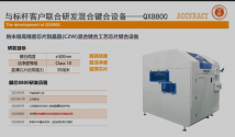
1691850134964.png

Before Hybrid Bonding, 2D, 2.5D and 3D packages all use solder bumps (solder bump) or micro bumps (Micro bump) to achieve chip and substrate, chip and interposer, chip and chip electrical connection. Hybrid bonding is an advanced stacking technique also known as direct bonding or cold bonding. This technology allows two chips to be directly connected together through metal, without the use of conventional solder or adhesives. It enables denser interconnects, shorter signal paths, and can increase bandwidth, reduce power consumption, and reduce manufacturing costs.

At present, Akris Qixin 8800 has achieved a bonding yield of 95% in the front-end wafer manufacturing line, and is striving to challenge higher bonding accuracy.

With the deceleration of Moore's Law, advanced packaging technology has become the new engine to promote the development of chip performance. BESI, a leading equipment manufacturer in the industry, believes that hybrid bonding technology is the key to the realization of advanced packaging technology, which can provide support for 2.5D/3D integrated architecture. At present, an important reason restricting the development of domestic advanced packaging is that the key equipment of advanced packaging has not yet achieved independent controllability.

Mr. Wang Chi, Chairman of Acres, said at the press conference that advanced packaging is a realistic path for my country's semiconductor industry to achieve cornering overtaking. The R&D and launch of Qixin 8800 is a breakthrough in the huge potential of the advanced packaging field.

With the support of the Jiangsu Provincial Department of Industry and Information Technology's key core technology and equipment research project funds, Akris chip-to-wafer high-precision hybrid bonding equipment has achieved a number of technological breakthroughs at nano-level precision, fully embodying Akris It has profound accumulation, excellent ability and strong determination in insisting on independent research and development capabilities, breaking through international technology blockades, overcoming difficulties, and creating value.

This press conference not only demonstrated the outstanding performance of Qixin 8800, but also highlighted the pioneering spirit of Akris in the cooperation of industry, university, research and application. Mr. Wang Chi introduced the Aike Research Institute to the guests, which is a joint development model and platform for production, education, research and application of Aike Ruisi and customers to jointly tackle key problems. He encouraged more customers to raise technical problems to promote the common progress of the industry. At the same time, he welcomed suppliers and partners to participate in tackling key problems, and jointly apply for projects with universities to provide more outstanding talents for the equipment industry.

This conference brought together more than 380 semiconductor equipment and core component companies, and discussed cutting-edge technologies and industry trends with the theme of "working together to seize opportunities, integrating innovation and manufacturing equipment". The launch of Qixin 8800 will undoubtedly arouse widespread attention inside and outside the industry in the strong atmosphere of the conference.

The release of Qixin 8800 will definitely bring new vitality and impetus to the industry. In the future journey, Acres will always keep its original intention and lead the semiconductor equipment - more accurate, faster and smarter.

Please, Log in or Register to view URLs content!
 

tokenanalyst

Brigadier
Registered Member

The first new office! Semiconductor Advanced Ceramic Materials Research Institute settled in Taixing High-tech Zone.​


The Institute of Semiconductor Advanced Ceramic Materials was jointly established by Taixing High-tech Zone, Jiangsu Provincial Industrial Technology Research Institute, Taizhou Industrial Technology Research Institute and the team of Professor Pan Wei of Tsinghua University. Focusing on the commonality and key technologies of the material industry, carry out industrial technology application research and integrated innovation, promote the transfer and transformation of scientific and technological achievements, derive and incubate technology-based enterprises, cultivate high-level innovative talents, and strive to build an international-level semiconductor ceramic material technology research and development center and industry base.

Relying on the State Key Laboratory of New Ceramics and Fine Technology of Tsinghua University, the Institute of Semiconductor Advanced Ceramic Materials has core products and patented technologies such as high thermal conductivity ceramic substrates and precision ceramic components for semiconductor equipment. It is at the world's advanced level and can meet the market demand for advanced ceramic components. Rigid demand for domestic substitution. The institute will focus on semiconductor key ceramic components, high thermal conductivity ceramic substrates, semiconductor ceramic powders, etc., to build a public technical service platform for powder research and development, process molding, sintering, and performance testing of semiconductor advanced ceramic materials, and to carry out industrial common and key research and development. Technology research and development, as well as the development and optimization of new ceramic preparation processes, strive to cultivate a number of high-tech companies and a main body to be listed during the construction period, and help the advanced ceramic industry to realize industrial cluster innovation and agglomeration development in Jiangsu and Taixing.


tphuang

Lieutenant General
Staff member
Super Moderator
VIP Professional
Registered Member
My notes from SMIC earnings call. Took me a long time to listen through this because I had to stop the playback multiple times to make sure I get the gist down. I think China's Semiconductor industry is lucky to have SMIC, because it is really tasked with a lot of responsibility. Many times, they stated that they have 10 platforms at each node in order to capture all the products and demands. Which makes sense given the need to have everything built locally. Anyhow, the good news is that both Jingcheng & Shenzhen have started mass production & SMIC is quickly building up volume to a breakeven point right now, especially with a lot of 28/40/55nm capacity

Lingang is building production line too and Tianjin is getting roofed now. Everything is coming together. Just needs more time. Demand for SMIC services in more advanced nodes (and even nodes that many westerners don't consider advanced like 55/65nm) are very high. This is not a problem that foreign fabs have to "deal with". SMIC really needs to ramp up quickly so that TSMC & UMC don't come in with their additional 28nm capacity and take everything

- no bright spot in consumer electronics and smart phone market, demand is decreasing, only automotive is a bright spot
- speed of de-stocking is slower than expected
- wafer increased 12% QoQ, but ASP decreased 7% due to change in product mix and price adjustment
- Time lapse in regional de-stocking. China region up to 80%
- inventory for some chips in consumer electronics & smartphones space for domestic customers have dropped
- they are re-stocking (CIS, ISP, high voltage drive, MCU, industrial control & specialty memory chips)
- Revenue from IoT/wireless routers declined due to reduced demand QoQ
- Capacity increased by 40k wpm 8-inch equivalent compared to beginning of year
- $1.7B capex in Q2, total $3B in first half
- Product inventory of main design company in China is gradually decreasing
- New product building inventory for end product shipment in H2 & next yr
- SMIC expect to gain market share in down cycle and achieve better revenue in H2
- China is largest IC/discrete market (35-40%), reconfiguration of supply chain -> more intense competition
- SMIC pursuing long term development, strengthen tech R&D to supply domestic industries, verify new product quickly
- standard/high volume products like DDIC, TDDI, CMOS major, CMOS major processor, specialty memory -> lower priced
- Unique/small volume product -> higher pricing
- When ramping up production, ratio of standard/high volume product is higher -> ASP lower
- for 8-inch fab, 3 major challenges cause prices to trend down/orders to shrink
- high volume PMIC for smartphone inventory too high
- Analog power market - IDMs really lower prices to compete w/ fabless designers
- LCD panel drivers crashing because of shrinking demand
- in H2, expect higher volume, higher utilization, but lower ASP
- Market for easy to do 8-inch wafer is high right now, commoditized chips
- > 10k different application of chips. Anyone that can do the most specialized/HQ products can control price
- SMIC is still small and can expand in unique product space, deliver customized tech for customers
- 8-inch capacity expansion has finished, believes when market comes back, capacity will be fully utilized
- Western customers often tier 1 suppliers on long term contract, so order reduction from end product didn’t happen until this yr
- As such, they are cutting orders 2 quarters after Chinese customers
- Chinese large/medium customers already restocking inventory for new products
- SMIC capacity planning does not change in medium/long term, but may slow down in short term based on customer demand
- SMIC’s capacity expansion right now based on new customer/products that are being demanded like in 28/40 nm space
- Need to expand in 28/40/55/65nm quickly to fulfill customer demand -> make sure SME purchases can meet customer demand
- Demand for standard logic 28/40 process is finite, so cannot just add capacity for standard products
- Products where SMIC was at 90/55nm like MCU, LCD driver & BCD, demand still exist in those markets
- But if SMIC can produce them at 40/28nm node, will gain customers in this space. 40/28nm are both good node for cost
- Need to whole suite of product in 28/40nm node. SMIC entered this segment later than market leaders like TSMC/Samsung
- But SMIC has many customers & many products -> will attract many customers when capacity is built up here
- Chinese customers picking up larger portion of supply chain orders -> causing full backlog for SMIC at 28/40/55nm nodes
- SMIC need to purchase certainly specialized equipment in order to fab specialized chips
- Refurbished smart phone market is huge & many Chinese suppliers in that market -> fabbing at SMIC
- capex required to build facility at Jingcheng/Lingang/Tianjin. Capex is higher now, but will bring returns later
- SMIC needs extra permission in ordering some SMEs, so need to order early to have enough SMEs for customers (in case some SMEs held up)
- SMIC is only 5% of market, so expansion will not change the market too much -> trying to calm investors abt large expansion plans
- The center market for 8-inch is 0.15/0.18 micron, most specialized products will not see gain moving to 0.13/0.11/90/65 node
- So demand for 8-inch will remain static for products like LCD drivers, BCD analog power, HV products
- power electronics for new energy product are all most well suited in 8-inch space
- For new node, SMIC starts with standard logic process and then expand to lower power, ultra lower power, RF, digital, analog, mixed signal, HV & others
- SMIC breaks field down to 10 platform, start with standard platform and then move to others. Like with Nor Flash now expanded to 55 & 40nm.
- 80% of process at each node is the same, developing platforms for additional products requires just some additional equipments
- Production line needs flexibility to handle different products from different lower volume, specialized customers to keep cost down
- JingCheng & Shenzhen 12-inch fab seeing most expansion this year, once SMEs installed, you need to ramp up production to keep cost down
- Lingang fab is building production line. Jingcheng installing more equipment, need to ramp up to breakeven production level asap

Now I need to listen to Huahong's earnings call. another long one!
 

weland

New Member
Registered Member
If it wasn't for the photovoltaic, power semiconductor and packaging industries, I think it will be safe to say that the Chinese semiconductor industry would be done for and therefore their IT and electronics industry. Because the close relation with the mainstream semiconductor industry these industries allowed many Chinese equipment and materials companies to survive and now because the market pressure of US export controls the are venturing their products more into the mainstream semiconductor industry.
A two prong approach I think could had been taken, using as much as possible domestic tools, materials and software for mature process, mems and so on and for edge node process import if necessary. That way, for example, SMEE KrF and ILine scanners would have develop more quickly.​
So I thank the U.S. it make many Chinese equipment and materials companies into mainstream semiconductor domestic tools . two prong approach i think it right .but Localization of third-generation semiconductors as soon as possible
 

tphuang

Lieutenant General
Staff member
Super Moderator
VIP Professional
Registered Member
My notes from Huahong earnings call

Huahong acquiring HLMC so that it doesn't compete against them is an interesting concept. Confirms my suspicion that they will face demand issues in the 90/65nm market, so have no choice but to move up to 40-55nm in order to capture the auto chip demand. New fab will be 83k just in phase 1! Wow, that means the plane here is pretty big too. Maybe they are planning to also add 200k wpm before end of this decade.
China Region revenue up 8.6% due to increased demand for IGBT, MCU, super junction
partially offset downturn from NOR Flash, CIS & PMIC products
Demand for NA down 1/3 due to decreased demand for PMIC
Demand for Asia down 22% due to general logic & MOSFET products
Demand for EU up 40% due to smart card ICs & IGBTs
Embedded NVM up due to MCUs & smart card ICs
standalone NVM down due to NOR Flash products
Discrete up due to IGBT & super junction products
Logic & RF down due to CIS & logic products
Analog & PM down due to other PMIC products

Capex $165m including $148.3m for Wuxi, $16.7m for 8-inch
12-inch capacity increasing (75-80k wpm now), look to reach 95k for next yr
Fully depreciated 8-inch fabs just print money
Higher depreciating cost on 12-inch, not fetching back enough revenue
Embedded NVM, nor flash and PMIC facing pricing pressure -> lower ASP (3-5% drop)
Logc & RF continue strong, IGBT & super junction doing well
Of 12-inch capacity, 1/3 to discrete, 30% for embedded NVM, 10% Nor Flash, 20-30 RF/PMIC


IPO money - mostly used to build next 12-inch fab (83k phase 1, $6.7B)
Remaining for R&D to improve product mix in 8-inch fab
Will acquire HLMC fabs over next 3 yrs so no competing business bw 2


Also based on their comment about NVM/Nor Flash vs SMIC, it's clear that SMIC's more advanced nodes allow them to capture certain higher paying customers. HH's website indicate they started producing 55nm embedded flash in 2021
Please, Log in or Register to view URLs content!

and they won't be able to move to 40nm until their new fab is build. So they can't compete for the same business that SMIC can. for example Gigadevice's MCU with 40nm nor flash
In September 2022, GigaDevice developed an automotive-grade MCU based on the Arm Cortex-M33 core, marking its entry into the car-use MCU segment. The first GigaDevice automotive MCUs, codenamed GD32A503, are manufactured using a 40 nm embedded flash memory process. GigaDevice's GD32A503 series of MCUs are suitable for developing automotive electronics applications, including body control modules, lighting, smart cockpits, ADAS, and power supplies.
 

olalavn

Senior Member
Registered Member
do you have any evidence of this? From what I hear, all their fabs are in Shenzhen like PXW & Swaysure
you should try to find who owns Ningbo fabs now...I once posted on twitter: they don't have to use their own fab...they get help from other companies...
 
Status
Not open for further replies.
Top