Chinese semiconductor industry

Status
Not open for further replies.

tokenanalyst

Brigadier
Registered Member

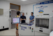
The unveiling ceremony of "Hangdian-Changchuan" semiconductor chip testing equipment laboratory was successfully held.​


School-enterprise cooperation to build laboratories is an important measure to cultivate innovative and application-oriented talents in the industry. On August 9, 2023, the unveiling ceremony of the "Hangdian-Changchuan" semiconductor chip testing equipment laboratory was successfully held at the Xiasha campus of Hangzhou Dianzi University. Li Wenjun, vice president of Hangzhou Dianzi University, Ni Jing, dean of the School of Mechanical Engineering, Zhong Fenghao, deputy general manager of Changchuan Technology, and Le Bin, deputy general manager of Changchuan Technology, attended the ceremony with representatives from both parties.​


1691768444569.png

Please, Log in or Register to view URLs content!
 

tokenanalyst

Brigadier
Registered Member

EUV mask model based on modified Born series​

State Key Laboratory of Intelligent Manufacturing Equipment and Technology, Huazhong University of Science and Technology, Wuhan, Hubei 430074, China
2Guangdong HUST Industrial Technology Research Institute, Guangdong Provincial Key Laboratory of Manufacturing Equipment Digitization, Dongguan, Guangdong 523003, China


Abstract​

Mask model is a critical part of computational lithography (CL). Owing to the significant 3D mask effects, it is challenging to accurately and efficiently calculate the near field of extreme ultraviolet (EUV) masks with complex patterns. Therefore, a method based on the modified Born series (MBS) was introduced for EUV mask modeling. With comparable accuracy, the MBS method was two orders of magnitude faster than the finite-difference time-domain method for the investigated examples. Furthermore, the time required for MBS was further reduced when the mask pattern was slightly changed. The proposed method shows great potential for constructing an accurate 3D mask model in EUV CL with high efficiency.

1691772262387.png

Fig. 1. (a) Schematic diagram of structure of EUV masks. (b) Computation process of the proposed model. The input of MBS consists of the incident field, pattern information and initial condition. The output of MBS is the diffraction field. It takes three steps to calculate the near fields of mask. MBS is used to calculate the downward diffraction. Then the reflection of multilayer is simulated by TMM. Finally, the near fields are obtained from the result of the upward diffraction.

4. Conclusion
In summary, we proposed a fast and accurate mask model for EUV CL. The model employs the SDM, in which the MBS is used to calculate the diffraction of the absorber, and the TMM is used to simulate the reflection of the multilayer. The results of MBS and FDTD are compared on logic, square array, line/space, and complex curvilinear patterns, which prove that MBS is a suitable alternative to FDTD in the application of the EUV absorber. For the investigated examples, a speed improvement of MBS versus FDTD by two orders of magnitude was observed and further speed advantage can be achieved on a GPU. In addition, the iterations of the MBS can be reduced by the initial condition from the field of the mask with a similar pattern. Considerable efficiency improvement of the MBS by the initial condition is demonstrated in three typical OPC situations, including hammerhead, mousebit, and SRAF, with various degrees of change in pattern, which is advantageous to OPC.

Compared with other mask models, the proposed model can simulate EUV masks with complex curvilinear patterns, and exhibits a good balance between speed and accuracy. The proposed mask model makes wide application of CL in EUVL closer. Although the results suggest several advantages, it is crucial to address some potential limitations. For example, MBS based on Fourier transform is difficult to implement parallelly for large-scale simulations. Besides, the discretization is too coarse to accurately represent the thickness. Further research is needed to overcome these limitations.

Please, Log in or Register to view URLs content!
 

tphuang

Lieutenant General
Staff member
Super Moderator
VIP Professional
Registered Member
Btw, I am a little disappointed that people are paying more attention to the link about America wanting china to be 5 generations behind rather than the link with q&a from smic earnings call.

That q&a really told me a lot.

At a time when fabs are having serious utilization issues in their more advanced processes, smic is not having any demand issues from 55nm and up. Everything is fully booked. Especially for 28/40 nm and I would imagine for finfet for sure.

Their existing 12-inch fab in Beijing simply isn't able to produce enough and they are trying to expand on it. More importantly, jingcheng fab has started mass production and same with Shenzhen and they are trying to increase 28 to 55nm capacity in both.

Demand is moving away from 90 to 65nm into nodes that require immersion equipment. Frankly, huahong is suffering from this move. It's going to be 2 yrs until their new fab can come online for 40nm stuff.

So right now, smic is capturing all the demand from domestic OEMs looking for domestic chip makers to de-risk.

One example of smic advancement is with nor flash. If you go to their website, it still shows 90 to 65nm as what they are capable of.
Please, Log in or Register to view URLs content!
But if you look at earnings call, they state that they have moved to 55 and then 40nm node for nor flash mass production.

Now, tsmc seems to have started mass production of 40nm back in 2018.
Please, Log in or Register to view URLs content!

So smic is unfortunately 5 years behind here. This is going to be a large and growing market given the increasing chip demand for cars.

And 28nm is the limit, so SMIC still has to get to that level to be more widely fab for embedded memories in auto chips.
Please, Log in or Register to view URLs content!
And based on this article, sounds like they have plenty of R&D work to do to gain in FRAM, MRAM & ReRAM. Not sure how far behind TSMC they are in all those areas.

Just think about Gigadevice, which is one of the largest customers of SMIC. They can seriously benefit from SMIC mass producing 40nm and then 28nm NOR Flash

So as SMIC get more capable in their processes, it will help domestic fabless and the efforts to do incorporate more domestic supply chain in end products
 

tokenanalyst

Brigadier
Registered Member
Please, Log in or Register to view URLs content!

can't really disagree with Gerald Yin here

“It’s a huge waste that a 1 billion yuan [US$138.7 million] ASML-made lithography machine has to wait for a domestically-made wafer coating and developing machine to catch up in speed,” Li said, referring to the Dutch chip equipment firm that has a virtual monopoly on the most advanced lithography machines.

An ASML lithography machine is capable of processing 350 12-inch wafers per hour, Li explained, while China-made wafer coating and developing machines cannot match that output.

well, wait no more.

1691790054168.png
 

sunnymaxi

Captain
Registered Member
its high time we should abandoned the SCMP for strategic industries news. they never fail to amaze me. always do post outdated information and deliberately choose someone for interview, who actually don't know where Chinese semiconductor tools makers currently stands..

you will be shocked if you read SCMP articles regarding Chinese turbofan engine development. misleading innocent people

disgusting reporting.
 

tokenanalyst

Brigadier
Registered Member
its high time we should abandoned the SCMP for strategic industries news. they never fail to amaze me. always do post outdated information and choose someone for interview, who actually don't know where Chinese semiconductor tools makers currently stands..
Is just lazy reporting and deceiving journalism, is pretty obvious that Li Jinxiang was referring to a past situation that already have been solved but the author framed Li as if he was talking in present tense.

Some of the reporters in SCMP are sometimes really lazy and deceiving when it comes to investigative journalism and they try to give their articles more depth that what you see in in the WSJ or Post but when you read the article is full of lazy reporting and the worst part is that they very rarely correct their articles.

The Digitimes maybe a Taiwanese bias talking point but credit where credit's due, they corrected their article about the ASML machine.
 
Status
Not open for further replies.
Top