Chinese semiconductor industry

Status
Not open for further replies.

FairAndUnbiased

Brigadier
Registered Member
Btw someone check my thinking on this (@tokenanalyst @FairAndUnbiased) but if your light source has high collimation and high coherence at point of generation that probably means you need fewer optical pass throughs to focus the beam for scanning right? And for each SD reduction in the collimation and coherence of the beam you probably need one factor multiple less in the number of optical passes? Because if so a 1 kW SSMB source might be able to adopt a simpler optics design and actually deliver some multiples more dosage at scanning point than a 1 kW LPP source, given that each optical pass translates to only 60-70% of the source power being transmitted to the next pass. Does that thinking check out?
LPP is incoherent and isotropic, thus you must have a collection mirror to minimize losses, and since it is very hard to get full collimation, beam transport will require multiple mirrors. The optics must be grazing incidence, which strongly limits the possible mirror geometries. That means its very difficult to have 100% collection just starting out.

Please, Log in or Register to view URLs content!

xraym04.jpg
xraym_s_003.jpg


EUV has very high interaction cross section with matter, thus all mirrors are strongly absorbing. Every additional mirror is ~30% loss.

Atomic-cross-sections-of-neutral-carbon-for-photoabsorption-elastic-scattering-and.png

So I indeed think that SSMB by virtue of high collimation and directionality already eliminates a major loss generator - the initial light collection.
 

ansy1968

Brigadier
Registered Member

AETHER

New Member
Registered Member
a writing from user “韭菜和瓜子” from 中国芯吧
Please, Log in or Register to view URLs content!


chatgpt translation:


the current situation as far as I know:

1. Most of the equipment for the 28nm process node can now be domestically produced. The main obstacle is the arfi duv lithography machine for the 28nm node. The initial prototype of this machine was taken offline in March 2022, and several units were produced by the manufacturer's laboratory and sent to some fabs for testing. According to sources, although it is a 28nm machine, testing must start from the 65nm process node, followed by 55nm, 45nm, and finally 28nm, progressing step by step. The current progress is unclear, but it is certain that the initial testing of the 55nm process node was achieved in the first quarter. These processes are very rigorous and must follow scientific principles. The sources also indicate that even for giants like ASML, it takes at least a year, if not more, to debug and optimize their new generation machines, whether it's DUV or EUV. The earliest possibility for the 28nm machine production line to be fully operational is the end of this year, while a slower timeline could be around mid-2024. The manufacturer is confident in their machine. Currently, the manufacturer's dry DUV machines are already in mass production and performing well with high demand. As a result, the manufacturer has started expanding production lines to prepare for mass production of arfi duv machines. According to sources, the expanded capacity will be 20 units per year.

2. 2. There is no fear of existing sanctions on machine equipment because some stockpiles have been accumulated in recent years. Even if there is an immediate complete decoupling from all Western countries, it would still be possible to sustain until domestic production of lithography machines is achieved.

3. The entire industry chain is not only focused on domesticating the machines but also localizing the machine components. Everyone is working diligently, and the progress is considerable. However, this does not mean that 100% completion has been achieved at the current stage. Fortunately, major domestic equipment manufacturers have also stockpiled many components in advance. Additionally, many of the components that have not been localized are general components, such as pipes, valves, pumps, seals, etc., which are not specifically developed for semiconductor equipment but widely used in various industrial equipment. These are the weak points of our industry, and many of these components are used in semiconductor equipment. However, since they are general supplies, it is difficult to impede their supply. Establishing a shell company or purchasing them in a third country is always an option.

4. Efforts are being made to address materials, electronic special gases, and semiconductor wet chemicals. The difficulty is, of course, less than that of machines, but there are hundreds of different types of materials and chemicals involved. For example, just for the arfi duv lithography resist, there are 20 or 30 types. Two years ago, Nanjing University of Science and Technology claimed to have sent two types of arf duv lithography resists for testing, which was merely an attempt to deceive outsiders. I previously posted a thread about lithography resists in the forum, and you can refer to that.

5. Process control software, robotic arms, mechanical hands, AMHS systems, and other related equipment are being developed by domestic manufacturers.

In summary, by 2025, a complete domestically produced 28nm production line can be established. After that, upgrades are planned every 12 months (not following Moore's Law's 18-month cycle), taking advantage of a late start and a determined technological direction without the need for exploration. In 2026, there will be a 14nm production line, followed by a 10nm line in 2027, and a 7nm line in 2028. The progress of EUV machines and EUV resists will become critical at that point, as other equipment is generally available.
 

tokenanalyst

Brigadier
Registered Member

Zuolan Microelectronics completed the B-round financing of nearly 100 million yuan to accelerate the deployment of mid-to-high-end filter series products​


A few days ago, Zuolan Microelectronics completed its B round of financing, led by Runke Fund, a subsidiary of China Resources. Previously, Zuolan Microelectronics has received investment from well-known institutions such as Shenzhen Pengchen Xunda, Wuxi Guolian Fund, Shenzhen Venture Capital, Zhengxuan Investment, and Yihe Capital . This round of financing will be used for new product research and development investment, market share increase and team building, and will further enhance the competitiveness and brand value of filter products.

Favored by capital, completed nearly 100 million yuan in round B financing
In the past 2022, due to the impact of events such as the slowdown of the macro economy and the complex and ever-changing international political situation, the capital market has become more cautious, and investment has focused on high-quality projects. Relying on its own hard-core strength, Zuolan Microelectronics is still recognized and supported by the capital market, and has obtained financing of nearly 100 million yuan, which further verifies that Zuolan Microelectronics has high investment value and future development expectations.
In the process of localization of RF front-end devices, the biggest difficulty encountered is insufficient technology accumulation resulting in insufficient forward design capabilities. Since the establishment of Zuolan Microelectronics, it has always maintained the original "core", focusing on technological innovation and enriching the product system. In the middle, adhere to the positive design technology route.
After each round of financing, Zuolan Microelectronics has invested a lot of manpower and financial resources in the research and development of the underlying technology. After years of technical precipitation, it now has strong forward design capabilities. Its self-developed modular design platform and design database, This enables the R&D team to quickly carry out device iterations and forward development of new products.
After seven years of business practice and continuous new product research and development, Zuolan Microelectronics’ RF front-end product series have gradually expanded from SAW, TC-SAW to PESAW, PEBAW, and then to RF front-end modules, and the application fields have also expanded from smartphones to base stations, Automotive electronics, Internet of things and other expansion. After the B round of financing, Zuolan Microelectronics will also speed up the development and iteration of new products, strive to improve the level of product differentiation, and create conditions for the next stage of breakthrough development.

Please, Log in or Register to view URLs content!
 

tokenanalyst

Brigadier
Registered Member

ZHONGKE KEYI PARTICIPATED IN SEMICON CHINA 2023 WITH SEMICONDUCTOR TESTING EQUIPMENT AND LOCALIZATION SOLUTIONS FOR CORE COMPONENTS​


In the semiconductor industry, testing equipment and core components play a vital role and are the key components to realize high-precision manufacturing and high reliability of semiconductor devices. As the only company in China that has been working in the field of scanning electron microscopes for more than 50 years, Zhongke Keyi has successfully developed a variety of scanning electron microscopes and developed the first field emission gun scanning electron microscope in China in recent years, breaking the monopoly of foreign technology and solving the problem of China's semiconductor and other high-end equipment manufacturing fields have a "stuck neck" problem of relying on imports of testing equipment, which is widely used in wafer testing, line width measurement, and semiconductor device failure analysis.

Vacuum environment is the basic condition of the semiconductor production process. Etching, ion implantation, thin film deposition, etc. in the semiconductor front-end process all need to be carried out in a vacuum environment. Vacuum products are the core components of semiconductor equipment. The magnetic levitation molecular pump is the ultra-high vacuum product with the highest technical level. Zhongke Keyi developed the first magnetic levitation molecular pump in China and formed a series of products. Among them, the semiconductor series magnetic levitation molecular pump has passed the approval of many leading semiconductor equipment manufacturers. Long-term rigorous process verification has achieved mass sales. At present, Zhongke Keyi has accumulated many years of product application experience in the field of semiconductors, and has a deep understanding of semiconductor process requirements. It can customize design and production according to customer needs to meet the localization of imported products and the use of domestic semiconductor equipment.

1688738404999.png

More confident about their EUV capabilities.

1688738790617.png

Please, Log in or Register to view URLs content!
 

siegecrossbow

General
Staff member
Super Moderator
a writing from user “韭菜和瓜子” from 中国芯吧
Please, Log in or Register to view URLs content!


chatgpt translation:


the current situation as far as I know:

1. Most of the equipment for the 28nm process node can now be domestically produced. The main obstacle is the arfi duv lithography machine for the 28nm node. The initial prototype of this machine was taken offline in March 2022, and several units were produced by the manufacturer's laboratory and sent to some fabs for testing. According to sources, although it is a 28nm machine, testing must start from the 65nm process node, followed by 55nm, 45nm, and finally 28nm, progressing step by step. The current progress is unclear, but it is certain that the initial testing of the 55nm process node was achieved in the first quarter. These processes are very rigorous and must follow scientific principles. The sources also indicate that even for giants like ASML, it takes at least a year, if not more, to debug and optimize their new generation machines, whether it's DUV or EUV. The earliest possibility for the 28nm machine production line to be fully operational is the end of this year, while a slower timeline could be around mid-2024. The manufacturer is confident in their machine. Currently, the manufacturer's dry DUV machines are already in mass production and performing well with high demand. As a result, the manufacturer has started expanding production lines to prepare for mass production of arfi duv machines. According to sources, the expanded capacity will be 20 units per year.

2. 2. There is no fear of existing sanctions on machine equipment because some stockpiles have been accumulated in recent years. Even if there is an immediate complete decoupling from all Western countries, it would still be possible to sustain until domestic production of lithography machines is achieved.

3. The entire industry chain is not only focused on domesticating the machines but also localizing the machine components. Everyone is working diligently, and the progress is considerable. However, this does not mean that 100% completion has been achieved at the current stage. Fortunately, major domestic equipment manufacturers have also stockpiled many components in advance. Additionally, many of the components that have not been localized are general components, such as pipes, valves, pumps, seals, etc., which are not specifically developed for semiconductor equipment but widely used in various industrial equipment. These are the weak points of our industry, and many of these components are used in semiconductor equipment. However, since they are general supplies, it is difficult to impede their supply. Establishing a shell company or purchasing them in a third country is always an option.

4. Efforts are being made to address materials, electronic special gases, and semiconductor wet chemicals. The difficulty is, of course, less than that of machines, but there are hundreds of different types of materials and chemicals involved. For example, just for the arfi duv lithography resist, there are 20 or 30 types. Two years ago, Nanjing University of Science and Technology claimed to have sent two types of arf duv lithography resists for testing, which was merely an attempt to deceive outsiders. I previously posted a thread about lithography resists in the forum, and you can refer to that.

5. Process control software, robotic arms, mechanical hands, AMHS systems, and other related equipment are being developed by domestic manufacturers.

In summary, by 2025, a complete domestically produced 28nm production line can be established. After that, upgrades are planned every 12 months (not following Moore's Law's 18-month cycle), taking advantage of a late start and a determined technological direction without the need for exploration. In 2026, there will be a 14nm production line, followed by a 10nm line in 2027, and a 7nm line in 2028. The progress of EUV machines and EUV resists will become critical at that point, as other equipment is generally available.

Looking forward to the day that semiconductor tech becomes junk tier tech just like lowbypass, high thrust turbofans.
 

tokenanalyst

Brigadier
Registered Member

The advanced computing power has achieved remarkable results, and the industry's first commercial mass-produced storage-computing integrated chip was unveiled at the World Artificial Intelligence Conference​


1688742562487.png
On July 6, the 2023 World Artificial Intelligence Conference (WAIC) opened at the Shanghai World Expo Center. The China Artificial Intelligence Industry Innovation Achievement Exhibition, as an important part of the conference, attracted many visitors. The exhibition focused on the research and development of cutting-edge technologies such as smart chips, large-scale models, and humanoid robots, as well as the application of scene demonstrations, presenting an active picture of artificial intelligence innovation and application to the audience. Among many cutting-edge technologies, the memory-computing integrated chip is considered to be the hottest architecture innovation direction in the field of AI chips, which can effectively solve the problems of "storage wall" and "power consumption wall" of traditional von Neumann architecture chips, and achieve a breakthrough in computing power .
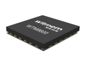
In the global storage-computing integrated market, some overseas manufacturers have deployed earlier. In 2017, the first batch of domestic storage-computing integrated chip companies represented by Zhicun Technology was established, which opened the commercial exploration of China's storage-computing integrated chips. In 2022, Zhicun Technology will take the lead in completing the mass production and shipment of SoC chips integrating storage and computing, and the financing will enter the B round. In January 2023, it will once again officially announce the completion of the B2 round of financing. At this World Artificial Intelligence Conference, Zhicun Technology focused on the application and commercialization of its SoC chip WTM2101, and at the same time brought the research and development progress of WTM series products with higher computing power.
The SoC chip WTM2101 with a shipment volume of one million is mainly used in terminal products such as TWS earphones, VR headsets, and smart watches. Noise, automatic environment recognition and other AI algorithms that have higher requirements on computing power and power consumption. It is reported that Zhicun Technology will also accelerate the application market of WTM2101 to spread to health equipment, medical equipment, industrial positioning and other scenarios.
 
Status
Not open for further replies.
Top