"Keep your enemies companies close and your domestic companies even closer"Given their governments intend to be an existential threat, it would be better not to give their companies any revenue at all...
You are using an out of date browser. It may not display this or other websites correctly.
You should upgrade or use an alternative browser.
You should upgrade or use an alternative browser.
Chinese semiconductor industry
- Thread starter Hendrik_2000
- Start date
- Status
- Not open for further replies.
Hantiancheng announced the mass production of 8-inch SiC epitaxial wafers, and has signed a long-term order of 129 million US dollars
Hantiancheng Electronic Technology (Xiamen) Co., Ltd. announced that the R&D team has completed the technical development of the 8-inch silicon carbide epitaxy process with independent intellectual property rights. Hantiancheng
Recently, Hantiancheng Electronic Technology (Xiamen) Co., Ltd. announced that the R&D team has completed the technical development of the 8-inch silicon carbide epitaxial process with independent intellectual property rights, and Hantiancheng has officially possessed the mass production capacity of domestic 8-inch silicon carbide epitaxial wafers .

It is reported that Hantiancheng completed the signing of a number of long-term contracts (LTAs) last week, including an 8-inch contract worth more than 192 million US dollars. The quality of the 8-inch silicon carbide epitaxial wafers produced by the company has reached the international advanced level, that is, the thickness non-uniformity is less than 3%, the concentration non-uniformity is less than 6%, and the yield rate of 2mm*2mm die reaches more than 98%.
This technological breakthrough marks that my country has mastered the commercialized 8-inch silicon carbide epitaxy growth technology, further promoted the localization process of silicon carbide epitaxy materials, and greatly enhanced my country's international status in the field of silicon carbide epitaxy.
According to Dr. Zhao Jianhui, chairman of Hantiancheng Company, in the semiconductor field, increasing the chip size is the best way to improve the competitiveness of semiconductor products. Taking a die with a size of 2mm*2mm as an example, through the exact same process, the chip (device) output of an 8-inch silicon carbide epitaxial wafer is 1.8 times that of a 6-inch wafer, which is 4-inch wafer output. 4.3 times. It can be seen that the introduction of 8-inch silicon carbide epitaxial wafer products will effectively reduce the cost of device production, which has far-reaching significance for promoting the development of the silicon carbide semiconductor industry.
Hantiancheng is currently the world's largest manufacturer of silicon carbide semiconductor pure epitaxial wafers, and it is a national-level specialized special new key "little giant" enterprise (the first batch in the first year). The company was established in Xiamen Torch High-tech Zone in March 2011. In March 2012, Hantiancheng became the first company in China to provide commercial 3-inch and 4-inch silicon carbide semiconductor epitaxial wafers. The products have reached the international advanced level and filled the gap in China. In April 2014, Hantiancheng completed the first commercial 6-inch silicon carbide epitaxial wafer order, becoming the first domestic and the fourth global manufacturer to provide commercial 6-inch silicon carbide epitaxial wafers. At present, Hantiancheng has reached the world's leading level in all product technical indicators. Based on the newly developed technology, Hantiancheng's high-uniformity product indicators can provide absolute competitive advantages for companies that produce automotive-grade main drive MOSFETs. This competitive advantage makes the 2023 annual order signed by Hantiancheng more than three times the annual production capacity of the original global leading company.
Hantiancheng's orders in hand (350,000 pieces) in 2023 will account for as high as 43.7% and 32.7% of the world. It is understood that most of Hantiancheng's Diamond Class epitaxial production capacity in 2024 has been locked by the LTA long-term contract. Hantiancheng serves the vast majority of silicon carbide semiconductor device companies in the Greater China region, and is the only epitaxial wafer manufacturer in the Greater China region that has entered the supply chain of international giants in large quantities. It also serves Infineon, STMicroelectronics, ON Semiconductor and Wolfspeed is the three international giants among the four global silicon carbide Top 4. The rapid development of Hantiancheng has also greatly promoted and improved the competitiveness of domestic silicon carbide semiconductor substrates in the international market.
Recently, Hantiancheng Electronic Technology (Xiamen) Co., Ltd. announced that the R&D team has completed the technical development of the 8-inch silicon carbide epitaxial process with independent intellectual property rights, and Hantiancheng has officially possessed the mass production capacity of domestic 8-inch silicon carbide epitaxial wafers .

It is reported that Hantiancheng completed the signing of a number of long-term contracts (LTAs) last week, including an 8-inch contract worth more than 192 million US dollars. The quality of the 8-inch silicon carbide epitaxial wafers produced by the company has reached the international advanced level, that is, the thickness non-uniformity is less than 3%, the concentration non-uniformity is less than 6%, and the yield rate of 2mm*2mm die reaches more than 98%.
This technological breakthrough marks that my country has mastered the commercialized 8-inch silicon carbide epitaxy growth technology, further promoted the localization process of silicon carbide epitaxy materials, and greatly enhanced my country's international status in the field of silicon carbide epitaxy.
According to Dr. Zhao Jianhui, chairman of Hantiancheng Company, in the semiconductor field, increasing the chip size is the best way to improve the competitiveness of semiconductor products. Taking a die with a size of 2mm*2mm as an example, through the exact same process, the chip (device) output of an 8-inch silicon carbide epitaxial wafer is 1.8 times that of a 6-inch wafer, which is 4-inch wafer output. 4.3 times. It can be seen that the introduction of 8-inch silicon carbide epitaxial wafer products will effectively reduce the cost of device production, which has far-reaching significance for promoting the development of the silicon carbide semiconductor industry.
Hantiancheng is currently the world's largest manufacturer of silicon carbide semiconductor pure epitaxial wafers, and it is a national-level specialized special new key "little giant" enterprise (the first batch in the first year). The company was established in Xiamen Torch High-tech Zone in March 2011. In March 2012, Hantiancheng became the first company in China to provide commercial 3-inch and 4-inch silicon carbide semiconductor epitaxial wafers. The products have reached the international advanced level and filled the gap in China. In April 2014, Hantiancheng completed the first commercial 6-inch silicon carbide epitaxial wafer order, becoming the first domestic and the fourth global manufacturer to provide commercial 6-inch silicon carbide epitaxial wafers. At present, Hantiancheng has reached the world's leading level in all product technical indicators. Based on the newly developed technology, Hantiancheng's high-uniformity product indicators can provide absolute competitive advantages for companies that produce automotive-grade main drive MOSFETs. This competitive advantage makes the 2023 annual order signed by Hantiancheng more than three times the annual production capacity of the original global leading company.
Hantiancheng's orders in hand (350,000 pieces) in 2023 will account for as high as 43.7% and 32.7% of the world. It is understood that most of Hantiancheng's Diamond Class epitaxial production capacity in 2024 has been locked by the LTA long-term contract. Hantiancheng serves the vast majority of silicon carbide semiconductor device companies in the Greater China region, and is the only epitaxial wafer manufacturer in the Greater China region that has entered the supply chain of international giants in large quantities. It also serves Infineon, STMicroelectronics, ON Semiconductor and Wolfspeed is the three international giants among the four global silicon carbide Top 4. The rapid development of Hantiancheng has also greatly promoted and improved the competitiveness of domestic silicon carbide semiconductor substrates in the international market.
China says it told the U.S. and Europe about the export controls in advance
BEIJING — China’s Ministry of Commerce said Thursday the country told the U.S. and Europe about this week’s export controls in advance.
China did so through “export control dialogue channels,” commerce ministry spokesperson Shu Jueting said in Mandarin, translated by CNBC.
China does not target any specific country with the restrictions, she said, reiterating their goal is to protect national security.
Spokesperson Shu said the ministry had yet to receive any applications for export licenses, and noted the rules don’t take effect until Aug. 1.
Huh, does this mean that the fibre laser for LPP is a go, then? At the very least, this does look like very nice progress.
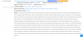
This paper is probably related to that patent. Same names. Same institutes. If they’re getting a conversion efficiency of 7% that is *nuts*.
That will mean three light sources possibilities. LPP (CAS), DPP 150W (Harbin) and SSMB (Tsinghua)1KW
This paper is probably related to that patent. Same names. Same institutes. If they’re getting a conversion efficiency of 7% that is *nuts*.
I think Harbin’s DPP is completely out of the picture at this point. If they’re getting a conversion efficiency of 7% with their LPP drive laser there’s a good chance they blow by SSMB’s 1 KW target. SSMB should still scale easier long term but the LPP instrument might get to adoption first.That will mean three light source probabilities, LPP (CAS), DPP 150W (Harbin) and SSMB 1KW
If this paper is correct and they can translate these results to a commercial instrument, heck if they can even get half this conversion efficiency at the drive laser power we’ve already heard them reach (20-30 kw) they are destroying the level of output even ASML’s next generation high NA instrument is supposed to be able to do. If these numbers are right when they finally get an EUV instrument I don’t think it will be like ASML’s entry instrument but an instrument that surpasses their whole product timeline.
Last edited:
Cleanness is another issue, DPP produce more debris but I don't know how advance is Harbin in this area, but in the other side DPP is the cheapest of the three.I think Harbin’s DPP is completely out of the picture at this point. If they’re getting a conversion efficiency of 7% with their LPP drive laser there’s a good chance they blow by SSMB’s 1 KW target. SSMB should still scale easier long term but the LPP instrument might get to adoption first.
If this paper is correct and they can translate these results to a commercial instrument, heck if they can even get half this conversion efficiency at the drive laser power we’ve already heard them reach (20-30 kw) they are destroying the level of output even ASML’s next generation high NA instrument is supposed to reach. If these numbers are right when they finally get an EUV instrument I don’t think it will be like ASML’s entry instrument but an instrument that surpasses their whole product timeline.
SSMB is ultraclean and doesn't require a colector mirror. In term of price Tsinghua says it could be cheaper than LPP per watt. But the concept for using SSMB,FELs and synchrotron radiation for EUV is relative new.
I think SSMB is the superior approach if you want scale but you need to put up upfront investment to support it because the whole fab process line is going to have to be reconfigured around that infrastructure. The problem with the technology is that it’s just not very portable. On the flip side upgrading just requires boosting the storage ring power, not a whole new instrument, and the scanners themselves can be upgraded independently of the instrument much more easily. You are probably going to get less transmission lose with SSMB as well, and the very tight emissions wavelength and beam collimation should help with scanning efficiency, and may even enable novel scanning strategies to get the most out of the scanner resolution. I think insofar as you expect large scale production of sub 10 nm chips going into the future SSMB is the better long term bet but if you get a working high power LPP first you don’t wait for it before you flash the green light.Cleanness is another issue, DPP produce more debris but I don't know how advance is Harbin in this area, but in the other side DPP is the cheapest of the three.
SSMB is ultraclean and doesn't require a colector mirror. In term of price Tsinghua says it could be cheaper than LPP per watt. But the concept for using SSMB,FELs and synchrotron radiation for EUV is relative new.
- Status
- Not open for further replies.

