Chinese semiconductor industry

Status
Not open for further replies.

tokenanalyst

Brigadier
Registered Member

GT400TL65P4H Photovoltaic and Energy Storage Solution​


The GT400TL65P4H (photovoltaic version) and GT400TL65P4H (energy storage version) launched by Yinmao Micro can be applied to 110kW 1000V system photovoltaic inverter and 120kW 1000V system energy storage inverter respectively, and can be applied to 1000V bus voltage. From the simulation results It can be seen that both schemes have good efficiency performance.

1688673122787.png


Please, Log in or Register to view URLs content!


tokenanalyst

Brigadier
Registered Member
To put things in perspective, a 6.9% conversion efficiency means to match the 1kW SSMB target, a 14.5kW fiber laser is needed. The Silent Hunter laser's output is 30kW.
I think it has to be a pulse laser and the pulse frequency of the laser has to match that of the target. I don't know if this military laser has these specs.
 
Last edited:

latenlazy

Brigadier
Btw someone check my thinking on this (@tokenanalyst @FairAndUnbiased) but if your light source has high collimation and high coherence at point of generation that probably means you need fewer optical pass throughs to focus the beam for scanning right? And for each SD reduction in the collimation and coherence of the beam you probably need one factor multiple less in the number of optical passes? Because if so a 1 kW SSMB source might be able to adopt a simpler optics design and actually deliver some multiples more dosage at scanning point than a 1 kW LPP source, given that each optical pass translates to only 60-70% of the source power being transmitted to the next pass. Does that thinking check out?
 

tokenanalyst

Brigadier
Registered Member
Btw someone check my thinking on this (@tokenanalyst @FairAndUnbiased) but if your light source has high collimation and high coherence at point of generation that probably means you need fewer optical pass throughs to focus the beam for scanning right? And for each SD reduction in the collimation and coherence of the beam you probably need one factor multiple less in the number of optical passes? Because if so a 1 kW SSMB source might actually deliver some multiples more dosage at scanning point than a 1 kW LPP source. Does that thinking check out?
SSMB will be laser like so a collector mirror or optics would not be necessary but it does need an optical path to reach the mask and the projection system and the objective system.

Pretty similar to the one they tested in 2017 but much power and advanced.

EUV technology testing platform from 2017, kinda like the concept. Looks suitable to test SSMB as a light source.

View attachment 97418View attachment 97419

Please, Log in or Register to view URLs content!

Please, Log in or Register to view URLs content!

General Research Laboratory of Microelectronics Equipment of the Institute of Optoelectronics has made breakthroughs in key unit technologies such as vacuum, film transport, workpiece table, vibration reduction and focus detection: the vacuum system achieves a stable high vacuum environment of 5.8 × 10 -7 Torr , ensuring that The stability of EUV light source propagation is improved; the frame and vibration reduction system of the whole machine meet the VC-F vibration reduction standard, and the vibration isolation effect is good in the frequency range of 2.2Hz - 500Hz in the horizontal direction and 2Hz- 500Hz in the vertical direction . The frame, workpiece table and mask table The stability meets the requirements of 32nm lithography and sub-nanometer wave aberration detection; the leveling and focusing detection system achieves nanometer-level detection accuracy, which provides a guarantee for the continuous multiple repetition of 32nm lithography resolution. At the same time, in the development of the workpiece table, the collaborative control technology of multiple workpiece tables is studied on the basis of the existing ones, which solves the problems of simultaneous control and position switching of the wafer table and the image table, the mask table and the object table; the automatic film feeding system Realize automatic loading and unloading in a vacuum environment ; the software system completes multi-module complex control, and coordinates each sub-system to complete the exposure process.

On the basis of completing the development of the key unit system, it has played a great role in cooperating with the overall project unit Changchun Institute of Optics and Mechanics to achieve 32nm repeatable exposure and with Shanghai Institute of Optics and Mechanics to achieve sub-nanometer wave aberration detection, which has been greatly affected by the overall project unit and each subject unit. And the acceptance group experts praised. During the research and development of the subject, the research group has achieved a series of original achievements in the fields of workpiece table control and precision measurement technology, and has applied for 31 invention patents , including 28 domestic patents and 3 international patents .
 

latenlazy

Brigadier
SSMB will be laser like so a collector mirror or optics would not be necessary but it does need an optical path to reach the mask and the projection system and the objective system.

Pretty similar to the one they tested in 2017 but much power and advanced.
If they can get SSMB to work that’s going to be such a game changer. This means a 1 kw SSMB light source is probably going to be able to deliver roughly an order of magnitude greater dosage than a 1 kw plasma produced light source. That’s an incredible scaling factor for the same output at source.
 

tokenanalyst

Brigadier
Registered Member
NAURA: Whaaat? your fab can't get the latest ASM epitaxial tool.
NAURA: Don't worry friend we have you cover.

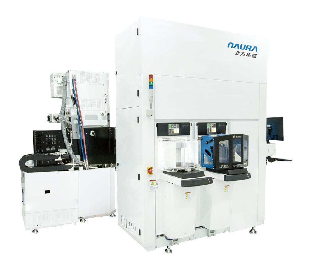
NAURA achieves full coverage of epitaxial process equipment


Release time: 2023-06-30

The manufacture of advanced chips requires nearly perfect crystal materials. Epitaxy equipment is the key equipment for growing crystal materials and is widely used in integrated circuits, power devices, silicon materials, third-generation semiconductors and other fields. As a pioneer of China's epitaxial process equipment technology, North Huachuang started the research and development of epitaxial equipment as early as 2010. After more than ten years of technological precipitation and innovative breakthroughs, more than 20 mass-produced epitaxial equipment have been released, and the cumulative shipments Nearly 1000 cavities.

Excellent product quality
Since the first silicon epitaxial equipment successfully entered the client in 2012, NAURA has formed a series of epitaxial equipment series products with core technology advantages and complete categories and wide applications. Capable of epitaxial growth technology for various materials: including monocrystalline silicon, polycrystalline silicon, silicon carbide (SiC), gallium nitride (GaN), indium phosphide (InP), etc., covering integrated circuits, power devices, radio frequency, semiconductor lighting and other fields Application requirements.


1688681270584.png
— NAURA Epitaxy Process List —
Achieve full coverage from 4 inches to 12 inches: including 8-inch and below single-chip and multi-chip large-capacity silicon epitaxy equipment, 12-inch silicon epitaxy equipment, 4/6/8-inch silicon carbide epitaxy equipment, 8-inch and below single-chip and Multi-chip GaN-on-Si epitaxial equipment with large capacity.


1688681396635.png
— 4-12 inch single-chip/multi-chip epitaxial equipment diagram —
Popular is well-known in the industry
With great efforts, after more than ten years of accumulation in technology and market, NAURA's epitaxy products have made remarkable achievements and have continuously won praise from customers and the industry. The company's first 8-inch silicon epitaxy equipment in the field of epitaxy broke the industry's competitive landscape and became the mainstream Baseline (benchmark) product in the industry, pushing the industry to a new level. Since its launch, it has almost won all orders from the domestic market.

The 12-inch atmospheric pressure silicon epitaxial equipment has broken through a series of key technologies and has been widely recognized by the market: in the field of power devices, it has continuously mass-produced more than 200,000 pieces at the client so far; The terminal has achieved stable mass production, and various key indicators have reached the international mainstream level. In addition, with its excellent process performance and market performance, the product won the fifth "IC Innovation Award" of China Integrated Circuit Innovation Alliance in 2022.

Facing the hot-invested silicon carbide field, North Huachuang has rapidly developed silicon carbide epitaxial products with its profound technology accumulation. At present, the products have achieved sales of nearly 200 units, accounting for half of the market. Facing the 8-inch silicon carbide market, NAURA's forward-looking 6/8-inch compatible multi-chip silicon carbide epitaxial equipment will soon be put into the market, which will greatly reduce customer operating costs and trigger a new round of market boom.

Innovative always research and always new
Since 2010, North Huachuang has benchmarked the cutting-edge technology of the industry, intensively studied the market and customer needs, and through continuous innovation, has broken through and optimized a series of airflow fields, heating fields, gas system systems, temperature control, pressure control, and motion systems. Key technologies, and customized research and development according to customer needs.

The multi-zone temperature control technology can improve the crystallization quality of the epitaxial layer, optimize the doping distribution of the epitaxial layer, and meet various technical requirements. High-temperature clean chamber technology can reduce crystal impurities and defects, improve the crystal quality of the device layer, and improve device performance. The multi-zone horizontal airflow field design realizes unidirectional laminar flow and no reverse flow turbulence, which can broaden the epitaxial process window, improve the quality of the epitaxial interface, and realize the controllability of the epitaxial film layer and the high performance of the device. The simulation technology of heating field and air flow field under normal pressure and reduced pressure has improved the design efficiency of the process chamber and provided theoretical support for solving specific problems.

North Huachuang will always adhere to the exploration and research of cutting-edge technology in the industry, and is committed to creating forward-looking professional technologies and solutions, creating value for customers with excellent epitaxy equipment and innovative professional services, promoting industrial progress, and creating infinite possibilities !

Please, Log in or Register to view URLs content!

Still NAURA needs to develop a tool for Silicon/Germanium.
 

tokenanalyst

Brigadier
Registered Member
Sales of 12-inch deep silicon etching machine break through 100 cavities, NAURA assists Chiplet TSV process development

Release time: 2023-06-30

As the size of transistors continues to approach the atomic scale, Moore's Law is slowing down. Faced with the increased cost and complexity of process technology, the market urgently needs to find another way to achieve high chip performance at low cost. TSV (Through Silicon Advanced packaging represented by Via (Through Silicon Via) technology has become an important way of chip integration. The 12-inch advanced packaging field PSE V300 launched by NAURA in 2020 has become the main machine of the domestic TSV mass production line because its performance has reached the international mainstream level and it has solid practical experience in being widely used in domestic 12-inch mainstream Fab factories.

64a5482c2333c.png

TSV technology is to make through-silicon holes between chips (Chip to Chip), between chips and wafers (Chip to Wafer), and between wafers (Wafer to Wafer), and then through thin film deposition, Metal filling, thinning, bonding and other processes realize the electrical interconnection of through-silicon vias. "TSV is the only technology that can realize the upper and lower interconnections inside the chip, and can enable multiple chips to achieve vertical and shortest interconnection" [1]. Among them, the production of through-silicon vias is one of the cores of TSV technology, which imposes strict requirements on the etching rate, aspect ratio, etching morphology, uniformity, and selection ratio of the etching process for producing through-silicon vias. , Because of this, TSV technology still has high technical barriers, and only a few domestic companies have mass production capabilities.

Through the fast gas and radio frequency switching control system, PSE V300 can accurately control the sidewall morphology in 50:1 high aspect ratio deep silicon etching, and realize no damage to the sidewall and no loss of line width; the excellent real-time control performance is greatly improved Etching rate, its TSV etching rate has reached the international mainstream level. In terms of structural system, PSE V300 adopts a single-chip design per cavity, and has excellent technological performance in terms of airflow field uniformity. The machine can be equipped with 6 chambers at the same time, which has excellent performance in ensuring mass production.

After three years of iterative updates, PSE V300 has gradually been applied to many fields such as power devices, image sensors and micro-electromechanical systems from the initial 2.5D/3D packaging field. In the future, NAURA will accelerate the pace of independent innovation, continuously promote the iterative upgrade of etching equipment, and provide more excellent solutions for more semiconductor technologies.​

Please, Log in or Register to view URLs content!
 

tphuang

Lieutenant General
Staff member
Super Moderator
VIP Professional
Registered Member
Please, Log in or Register to view URLs content!
this is a little disappointing to read
而从国外情况看,Wolfspeed、ROHM、英飞凌、ST等国际碳化硅大厂已经纷纷迈入8英寸,这些厂商的量产节点也纷纷提前到今年。值得一提的是,前文所述意法和三安光电的合作主要集中在8英寸,英飞凌与两家国产SiC企业签订长约也表明未来将向8英寸进发。这有助于我国在碳化硅进展上加速赶上国际步伐。

8英寸是国内外厂家都想迅速攻下的堡垒,但良率问题始终是一座跨不过的大山。龚瑞骄表示:“目前6英寸SiC衬底国内的良率大概有40%,海外大概60~70%,在8英寸方面,近年来国际大厂积极推进8英寸产线建设,现阶段仅Wolfspeed一家步入量产,且实际进展并不如预期。”
looks like the tech of domestic SiC wafer manufacturers are still behind the Western companies.

It's just 40% yield on 6-inch SiC vs 60-70% abroad. Wolfspeed has now started mass production of 8-inch. So Chinese players definitely need to make improvements all around.
 
Status
Not open for further replies.
Top