Chinese semiconductor industry

Status
Not open for further replies.

GiantPanda

Junior Member
Registered Member
I'm now thinking about the billions of dollars each year that the Chinese government poured in to the semiconductor industry over a period of two decades with very meager returns at best. Its a good thing that they keep at it all those years or China would have to start from even further from behind in 2018 when the tech war started.

Those "billions" are pretty much peanuts in the grand scheme of things. But they keep an industry in being. The reason China has a firm in nearly every step of the entire semicon process is because there was just enough money to allow firms to develop in those niches despite crushing pressure from foreign competition.

Without that money, the vast majority of the pipeline would have no domestic companies to step in. This is actually the norm for every other country in the semicon business except maybe for Japan.
 

tphuang

Lieutenant General
Staff member
Super Moderator
VIP Professional
Registered Member
Please, Log in or Register to view URLs content!

Shanghai Jita's 12-inch BCD process has taped out and verified to satisfy criteria needed for mass production.

Jita works with Empyrean & Geely.

The entire project seems to be very big as we see constant bidding regarding to it
Please, Log in or Register to view URLs content!

looks like just 12-inch portion required 26B RMB investment for 50k wpm. 8-inch portion will be 110k wpm & another 30k wpm of SiC
 

Top water

Just Hatched
Registered Member
Those "billions" are pretty much peanuts in the grand scheme of things. But they keep an industry in being. The reason China has a firm in nearly every step of the entire semicon process is because there was just enough money to allow firms to develop in those niches despite crushing pressure from foreign competition.

Without that money, the vast majority of the pipeline would have no domestic companies to step in. This is actually the norm for every other country in the semicon business except maybe for Japan.
 

Franklin

Captain
Those "billions" are pretty much peanuts in the grand scheme of things. But they keep an industry in being. The reason China has a firm in nearly every step of the entire semicon process is because there was just enough money to allow firms to develop in those niches despite crushing pressure from foreign competition.

Without that money, the vast majority of the pipeline would have no domestic companies to step in. This is actually the norm for every other country in the semicon business except maybe for Japan.
That's my point those billions invested all those years means that China atleast have a minimum basic competency in semiconductor production on all levels. Without that China will really be in trouble today.
 

henrik

Senior Member
Registered Member
Those "billions" are pretty much peanuts in the grand scheme of things. But they keep an industry in being. The reason China has a firm in nearly every step of the entire semicon process is because there was just enough money to allow firms to develop in those niches despite crushing pressure from foreign competition.

Without that money, the vast majority of the pipeline would have no domestic companies to step in. This is actually the norm for every other country in the semicon business except maybe for Japan.

There was always enough money for semiconductor research. Compare to the excess investment in apartments, the money is just small amount.
 

Eventine

Junior Member
Registered Member
Investing in apartments was and is a market decision. Investing in chips was and is a strategic decision. You were never going to convince the average Chinese to blow their savings on chips investments. This had to be a government investment because like all strategic industries, it wouldn't have gotten any where without government intervention.

It's also why Western governments and institutions heavily promote market economics for developing countries - because they know countries that rely on the market can never hope to compete with Western superiority in technology.
 

antiterror13

Brigadier
I'm now thinking about the billions of dollars each year that the Chinese government poured in to the semiconductor industry over a period of two decades with very meager returns at best. Its a good thing that they keep at it all those years or China would have to start from even further from behind in 2018 when the tech war started.

yeahhh, if it was 10 yrs earlier, would be much more difficult for China
 

tokenanalyst

Brigadier
Registered Member

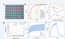
Microelectronics Institute makes progress in phototransistor-adaptive reservoir computing​

Edge artificial vision systems have become a research area that has attracted much attention due to their extensive applications in scenarios such as autonomous driving, smart home, and video surveillance. Due to the traditional artificial vision system adopting the " sensing - storage - computing " separation architecture, the frequent migration of a large amount of redundant sensing data between different modules leads to high system delay and high power consumption. One of the important ways to solve this problem is to develop an intrasensory or near-sensing computing artificial vision system that integrates sensing, storage and processing with neuromorphic computing technology. Pool computing is a neuromorphic computing technology with low computational complexity and low energy consumption. It is very suitable for combining with sensors and applied to edge terminals with limited resources. However, due to the fixed weight of the storage pool, while reducing the training cost, its network adaptability is limited, and it is difficult to apply to complex and changeable actual environments.
  To solve this problem, researcher Shang Dashan from Academician Liu Ming's team of the Key Laboratory of Microelectronic Devices and Integrated Technology of the Institute of Microelectronics cooperated with Dr. Based on the photoelectric nonlinear response mechanism and dynamic characteristics of MoS 2 field effect tube ( FET ), combined with the horizontal cell feedback mechanism in the biological vision system, a sensor-computing integrated time-delay storage pool computing technology with bright / dark light adaptive function was developed .

1687740903046.png

Please, Log in or Register to view URLs content!
 

tokenanalyst

Brigadier
Registered Member

Semiconductor Institute has made important progress in the research of silicon-based epitaxial quantum dot lasers​


Recently, the research team of Yang Tao and Yang Xiaoguang from the Materials Science Key Laboratory of the Institute of Semiconductors has made important research progress in silicon-based epitaxial quantum dot lasers and their doping regulation.
Silicon-based optoelectronic integrated chips are based on mature, highly integrated, and low-cost CMOS technology, and integrate a large number of functional devices required by traditional optical systems on the same chip at high density, greatly improving the information transmission and processing capabilities of the chip , can be widely used in emerging fields such as ultra-large data centers, 5G, Internet of Things, supercomputers, and artificial intelligence. Due to the low luminous efficiency of silicon (Si) materials, epitaxy of III-V semiconductor materials with high luminous efficiency such as gallium arsenide (GaAs) on a CMOS-compatible Si-based substrate, and the epitaxy and preparation of lasers are recognized as optimal On-chip light source solution. Due to the large lattice mismatch, polarity mismatch and thermal expansion coefficient mismatch between Si and GaAs materials, the development of high-performance silicon-based epitaxial lasers needs to solve a series of key scientific and technical difficulties.

Recently, the research team of Yang Tao and Yang Xiaoguang from the Materials Science Key Laboratory of the Institute of Semiconductors has made important research progress in silicon-based epitaxial quantum dot lasers and their doping regulation. The team used molecular beam epitaxy technology to reduce the defect density of silicon-based GaAs materials to the order of 106cm-2 under the condition that the total thickness of the buffer layer is 2700nm. The stacked InAs/GaAs quantum dot structure is used as the active region, and the domain-divided double doping control technology of "p-type modulation doping + direct Si doping" is proposed and applied to the active region for the first time, and a high-temperature working low-power on-chip light source. At room temperature, the continuous output power of the device exceeds 70mW, and the threshold current is 30% lower than that of the p-type doped laser with the same structure. The maximum continuous operating temperature of the device exceeds 115°C, which is the highest value of similar devices in public reports so far. The above technologies and results provide a key solution and core light source for realizing ultra-low power consumption, high temperature stable high-density silicon-based optoelectronic integrated chips.

Please, Log in or Register to view URLs content!
 
Status
Not open for further replies.
Top