Chinese semiconductor industry

Status
Not open for further replies.

european_guy

Junior Member
Registered Member
I have to dig up where I got the information from but the number of ascend developers have grown from under 100k in 2020 to 1.5 million now. I think all because Huawei came out with ascend 910 back in 2019. And since it was far and away the most competitive domestic GPU back then, all the developers gravitated to it and now ascend has dominant position in all the smart city projects.

So it is incorrect to say that all Chinese GPU makers are like AMD imo.


Slow down....

This is all going to take time. I think any de Americanized 14nm line in smsc will take some time to be fully tested and validated and brought up to par in yields and such. We should hold no illusion to that.

Again, I expect a test line set up this year but much of the expansion will probably happen next year

IIRC from Havoc thread, within April this year the 28nm DUVi should be fully assembled and tested in-house, then delivered to customer for validation (1 year time, more or less). In the meantime SMEE plans to deliver around 9 machines within 2024, but not the DUVi ones.

My personal opinion is that if the ASML ban turns true, this will translate in couple of years hole in the sub-28nm capacity development...maybe less if SMEE (and its customers) make a miracle with the DUVi's debugging process. Actually could be two yearish for 28nm in volume production, and another 2 to reach the 7nm. Anything less then this would be a China miracle....not that China is not able to make miracles, already did many.
 
Last edited:

paiemon

Junior Member
Registered Member
I have to dig up where I got the information from but the number of ascend developers have grown from under 100k in 2020 to 1.5 million now. I think all because Huawei came out with ascend 910 back in 2019. And since it was far and away the most competitive domestic GPU back then, all the developers gravitated to it and now ascend has dominant position in all the smart city projects.

So it is incorrect to say that all Chinese GPU makers are like AMD imo.
Yea I didn't intend that as a broad statement to apply t o all Chinese GPU makers since they stand across a spectrum in terms of capability, broad vs. narrow purpose but it was more of a statement regarding their relative competitive positions vis-a-vis AMD back when it was trying to catch up to Nvidia.
 

tokenanalyst

Brigadier
Registered Member
The only source on the development of a 28nm DUVi machine from China that I can find is this article headline and its from a Taiwanese publication. Unfortunately the article is behind a paywall.

Please, Log in or Register to view URLs content!
That is just photoresist not the machine itself, you will find more information in patents, companies own financial statements (Sina finance or investment sites) and research papers than in the press.
 

Strangelove

Colonel
Registered Member
Please, Log in or Register to view URLs content!

Semiconducting nanomaterial for curves holds promise for Internet of Things and wearables, says Hong Kong-led team​


  • Scientists say nanomesh can be made at much lower temperatures than existing semiconductors and on common materials such as paper and plastic
  • The researchers used tellurium, a semi-metallic element that can be mixed with other metals to form alloys


Please, Log in or Register to view URLs content!
Published: 6:02pm, 23 Jun, 2023 Updated: 6:32pm, 23 Jun, 2023


A team of Hong Kong-led scientists have developed a new way to produce a semiconducting nanomaterial that say can be made into sensors on curved surfaces to create safer infrastructure and advance flexible
Please, Log in or Register to view URLs content!
.

They said the nanomesh – formed from a network of nanowires – could be manufactured at much lower temperatures than for existing
Please, Log in or Register to view URLs content!
and grown on common materials such as plastic and paper, reducing production costs.

The team from City University of Hong Kong, the Changchun Institute of Optics, Fine Mechanics and Physics at the Chinese Academy of Sciences, the University of Electronic Science and Technology of China, Zhengzhou University, Beijing University of Technology and Kyushu University in Japan published their findings in the peer-reviewed journal Nature Communications in April.

Semiconductors are silicon-based devices made up of hundreds of millions, and in some cases billions, of transistors, which act as tiny “switches” to control the movement of electrons.

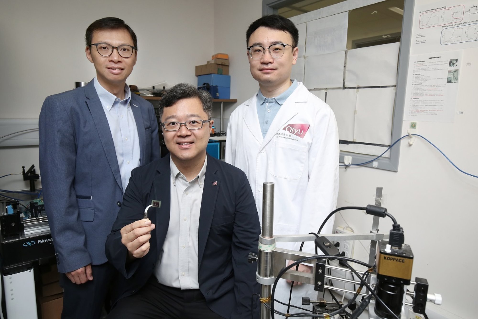
CityU’s research team (from left) Dr Alex Wong Chun-yuen, Professor Johnny Ho Chung-yin and Dr Meng You. Photo: Handout


CityU’s research team (from left) Dr Alex Wong Chun-yuen, Professor Johnny Ho Chung-yin and Dr Meng You. Photo: Handout
A semiconductor conducts electricity under some conditions but not others, making it a good medium to control electrical current. Most of the world’s semiconductors, also known as integrated circuits or microchips, are made from pure elements such as silicon extracted from sand.

In the recent study, the researchers used tellurium, an emerging semiconductor material. The element is semi-metallic – it can be controlled to act as a metal or semiconductor. It can be mixed with other metals to form alloys.
Lead author Johnny Ho Chung-yin, a professor in the department of materials science and engineering at CityU, said tellurium had a unique structure made up of spiral chains of atoms bonded by van der Waals force.

The force enables tellurium nanomeshes to self-weld and grow on rigid, flexible or curved surfaces. The self-welding process boosts the performance and mechanical robustness of electrical devices, according to the study.

“Thanks to van der Waals forces, we can grow the nanomesh on any substrate without worrying about defects in the material that could arise from being grown on an unsuitable substrate,” Ho said.

To create the nanomesh, the team first vaporised tellurium source powders and carried them to a base material, such as silicon oxide, polymers (stretchable plastics) or paper, where they were heated at 100 degrees Celsius (212 Fahrenheit) and grew. The temperature is far lower than the required 600 to 700 degrees using conventional methods.

Ho said the nanomaterial was promising for applications in the
Please, Log in or Register to view URLs content!
(IoT) – the network of physical objects embedded with sensors, software and other technology to collect and share data.

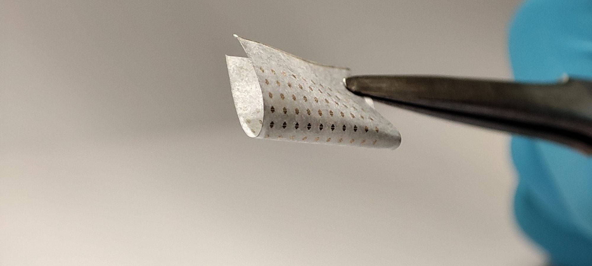
Low-cost nanomesh infrared photodetectors fabricated on paper. Photo: Dr Meng You, City University of Hong Kong.


Low-cost nanomesh infrared photodetectors fabricated on paper. Photo: Dr Meng You, City University of Hong Kong.

“Sensors can now be made with a flexible material for them to be deployed on curved surfaces like parts of a bridge. We can deploy sensors – as many as needed because they can be manufactured at low costs – to measure the amount of pressure the bridge bears, alert staff to areas where repair work is needed and ensure its safety,” Ho said.

He added that the data collected could be analysed in real time to reflect the structural safety of infrastructure and aircraft.

The nanomesh could also be used to build night-vision cameras which emit infrared light that is reflected off objects and detected by their sensors, Ho said.

Alex Wong Chun-yuen, an associate professor of chemistry at CityU who co-leads the research, said the cross-disciplinary project started when Ho, his long-time collaborator in material sciences, raised an issue that could potentially be addressed by the field of chemistry.

“As chemists we study the characteristics of the elements and are capable of manipulating the reaction conditions of the basic material,” he said, adding that his synthetic chemistry team helped ensure the manufacturing process could be replicated.

The team said they would continue to work on the nanomaterial and were experimenting with creating metal alloys with tellurium.
 

tphuang

Lieutenant General
Staff member
Super Moderator
VIP Professional
Registered Member
IIRC from Havoc thread, within April this year the 28nm DUVi should be fully assembled and tested in-house, then delivered to customer for validation (1 year time, more or less). In the meantime SMEE plans to deliver around 9 machines within 2024, but not the DUVi ones.

My personal opinion is that if the ASML ban turns true, this will translate in couple of years hole in the sub-28nm capacity development...maybe less if SMEE (and its customers) make a miracle with the DUVi's debugging process. Actually could be two yearish for 28nm in volume production, and another 2 to reach the 7nm. Anything less then this would be a China miracle....not that China is not able to make miracles, already did many.
pretty sure DUVi has already been delivered for testing/validation. He said DUVi is used for ICRD's 55nm line. My guess is that SMIC already testing with its prototype.

They will have SMEE DUVi in 28nm production process next year in all likelihood. The question is whether or not they will also have one for 14nm process.

I don't really seem why there will be a couple of years hole in sub-28nm development. They have stocked up 2050i scanners and can continue to buy 1980i and 1970Di. Although at this point, SMIC should also be stocking up as many 1980i and 1970Di as possible.

The way I look at ASML is this. It's the most important equipment of the entire process, so you want to first validate other domestic 7/14nm tools with ASML scanners while you work on improving SMEE scanner.

So, last yr, verified you can do ASML scanner + other domestic equipments for 40nm
This yr, you do the same for 28nm and 14nm (trial for 14nm at least) while starting validation of SMEE scanner w/ other domestic equipment for 28/40nm
Next yr, you do ASML + domestic for 7/14nm & complete validation of all domestic 28/40nm process + aim to also do it for 14nm
2025, w/ 2050i/2100i that you stocked up, you mass produce 5/7nm + aim for all domestic 7nm process, but at minimum mass producing 12/14nm with all domestic tools

you see at this point, SMEE DUVi is far more important to get right than any other scanners, since full ban of ASML DUVi scanners is a real possibility.

Yea I didn't intend that as a broad statement to apply t o all Chinese GPU makers since they stand across a spectrum in terms of capability, broad vs. narrow purpose but it was more of a statement regarding their relative competitive positions vis-a-vis AMD back when it was trying to catch up to Nvidia.

That's fine. I just want it to be clear that China does have a Nvidia already, it's Huawei/Hisilicon. Some of its competitors are reluctant to use its GPUs due to competition reasons, but full cut off to Nvidia GPUs would not be a big problem. It would just stimulate Hisilicon's dominant position in China
 

gelgoog

Lieutenant General
Registered Member
Huawei/HiSilicon does not design GPUs. They design CPUs for servers and NPUs for AI. All GPUs they used in smartphone SoCs were licensed.
There are lots of other NPU makers in China like Biren or Cambricon. Basically every major cloud provider also has their own design.

China does have GPU designers however like Moore Threads or Jingjia Micro. Chinese investors also own UK GPU designer Imagination Technologies (the designers of PowerVR architecture), and US GPU designer Vivante (owned by Chinese VeriSilicon).
 

tphuang

Lieutenant General
Staff member
Super Moderator
VIP Professional
Registered Member
Huawei/HiSilicon does not design GPUs. They design CPUs for servers and NPUs for AI. All GPUs they used in smartphone SoCs were licensed.
There are lots of other NPU makers in China like Biren or Cambricon. Basically every major cloud provider also has their own design.

China does have GPU designers however like Moore Threads or Jingjia Micro. Chinese investors also own UK GPU designer Imagination Technologies (the designers of PowerVR architecture), and US GPU designer Vivante (owned by Chinese VeriSilicon).
Given the context of the discussion, it was referring to AI chips in China, which they have with Ascend-910, which works the same as GPGPU. Biren also calls their AI chip GPGPU
 

tokenanalyst

Brigadier
Registered Member
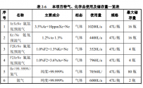
Some info from the public environmental report of RSLaser, looks like that the project for the mass production and refurbishing of high power high repetition rate KrF, ArF, ArFi excimer lasers, given the size scope of this project, is to mass produce a decent quantity of excimer laser powered lithography machines every year, I don't know how much of each type of litho machine the market leader in China, ASML, sells in China, but this annual production needs to come at the expense of someone else, RSLaser, Guowang Optical and CheerTech cannot have a sizable annual production of subsystems and not sell. it will make no sense.

Another thing is that ASML certificate these companies as suppliers for the Chinese market.​

1687555345955.png1687555551369.png
 
Status
Not open for further replies.
Top