Chinese semiconductor industry

Status
Not open for further replies.

tokenanalyst

Brigadier
Registered Member

The Institute of Microelectronics of the Chinese Academy of Sciences has made important progress in the field of semiconductor device physics​


The specific physical reasons for the widely exhibited nonlinear volt-ampere (IV) characteristics of semiconductor devices at low temperatures have been one of the most widely concerned topics in the past two decades. Previously, most studies attributed the nonlinear IV characteristics to the uniform modulation effect of the electric field on the electronic transition rate in semiconductor materials. This explanation not only failed to solve the problem of nonlinear transport, but also sparked more intense debates...
Due to the widespread disorder factors such as defect states in semiconductor devices, the transport of carriers often takes the form of transitions. Due to the complex types of defect states in semiconductors, it has always been a difficult and important topic in this field to accurately understand and describe the carrier transport and macroscopic electrical properties in semiconductor devices.
The specific physical reasons for the nonlinear volt-ampere ( IV ) characteristics widely exhibited by semiconductor devices at low temperatures have been one of the most widely concerned topics in the past two decades. Previously, most studies attributed the nonlinear IV characteristics to the uniform modulation effect of the electric field on the electron transition rate in semiconductor materials. This explanation not only did not solve the problem of nonlinear transport, but caused more intense debates (Nat. Mater. 8, 572(2009); Phys. Rev. Lett. 105, 156604 (2010)).
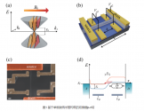
In response to such problems and debates, the team of academician Liu Ming from the Key Laboratory of Microelectronic Devices and Integrated Technology of the Institute of Microelectronics proposed the physical mechanism of the "collective transport" of carriers from a theoretical perspective. The theory holds that the non-uniform distribution of percolation path growth caused by the external electric field produces a collective transport effect, which in turn leads to nonlinear IV characteristics at the device scale. In terms of experiments, the team further realized the control of the percolation threshold of the device by skillfully controlling the dimension of the semiconductor in the polymer device. On this basis, it was directly confirmed that the nonlinear transport comes from the collective transport by controlling the nonlinear degree of the device IV . this assumption. This work unifies various hypotheses that have been controversial on this topic, and provides a theoretical basis for the development of methods to manipulate the I - V characteristics of semiconductor devices.

 

tokenanalyst

Brigadier
Registered Member

Peking University has made important progress in the study of carbon nanotube gate-controlled quantum interference effect.​


As an ideal low-dimensional electronic system, carbon nanotubes have a unique energy band structure and a high mean free path of carriers, and exhibit excellent quantum properties at low temperatures, showing great promise for the development of high-performance integrated circuits and solid-state quantum devices. tempting prospect. In mesoscopic devices, achieving a deep understanding and precise control of quantum interference effects is not only beneficial to the study of quantum coherence phenomena in low-dimensional electronic systems, but also lays the foundation for the development of new nanoelectronic devices and quantum devices. Carbon nanotubes are tubular one-dimensional crystals composed of carbon atoms, which provide an ideal experimental platform for studying the Aharonov-Bohm (AB) effect under an axial magnetic field. However, due to its ultra-small diameter, an ultra-high magnetic field is required to realize a magnetic flux quantum in carbon tubes (10nm diameter requires about 50T axial magnetic field), which greatly limits the experimental observation and research. Early experimental research used large-diameter multilayer carbon nanotubes to reduce the magnetic field required for the flux quantum, or through the Schottky barrier formed at the interface between carbon nanotubes and electrodes, using barrier tunneling to observe AB oscillations, However, it is difficult to overcome the inherent disorder of the system and the fixed tunneling barrier, so there is no stable and controllable means to study the AB effect in the one-dimensional system. In 2004, Andreev theoretically proposed that using the characteristic structure of the pn junction, by combining Landau-Zener tunneling with the AB effect, it is possible to observe the quantum interference effect of magnetic flux modulation at low field (Phys. Rev. Lett. 2007 , 99 , 247204), but it has not been realized experimentally due to the difficulty of device regulation.

Zhang Zhiyong and Kang Ning's research group from the School of Electronics, Peking University, Carbon-based Electronics Research Center, and the Key Laboratory of Nano-device Physics and Chemistry of the Ministry of Education cooperated with Wang Yin's team from Hongzhiwei Technology Co., Ltd. and Jiang Kaili's research group from the Department of Physics, Tsinghua University. Progress has been made in the research direction of quantum coherent transport of carbon nanotubes: the quantum interference effect regulated by the built-in electric field has been realized for the first time, and the AB effect enhanced by Fabry-Perot (FP) interference has been further observed in the low magnetic field region. By building a paired side gate structure on the chip, the research team realized the effective regulation of the pn junction strength of a single carbon nanotube, and obtained a high-quality carbon nanotube device working in the ballistic transport region (Figure 1). By stabilizing the working region of the device at the pn boundary in the double grid, the experiment successfully observed the characteristic non-monotonic magnetic transport behavior along the direction of the built-in electric field enhancement, which is consistent with the theoretically predicted image (Fig. 2a-c ). The AB origin of the magnetic permeability is further confirmed by the evolution behavior of magnetic transport at different dips at low temperature (Fig. 2b and Fig. 2d). This non-monotonic magnetic transport behavior was observed for the first time to be greatly enhanced in the resonance region of the FP (Fig. 2e), and the calculation method based on non-equilibrium Green's function and density functional further revealed the resonance-modulated transmission coefficient behavior (Fig. 2f). This work provides a new solution for the study of quantum interference effects in one-dimensional electronic systems and the development of multi-field control methods.

1685891253156.png


tokenanalyst

Brigadier
Registered Member
Haina Semiconductor Silicon Monocrystalline Production Base Project: The main body of the first-phase monocrystalline plant is fully capped


According to news from Jiwei.com, on June 4, new progress came from the Haina Semiconductor silicon single crystal production base project located in Yangqu Industrial Park, Shanxi Comprehensive Reform Demonstration Zone.
According to news from Shanxi Comprehensive Reform Demonstration Zone, recently, the steel structure roof of the monocrystalline plant building in Haina Semiconductor Silicon Monocrystalline Production Base Project (Phase I) in Yangqu Industrial Park, Shanxi Comprehensive Reform Demonstration Zone has been capped. So far, all the main bodies of the monocrystalline plant have been capped. The construction workers are stepping up construction and sprinting towards the start of production in August.
"Currently, the fine decoration of the comprehensive building has been completed, and the exterior wall construction is in progress; the dormitory building is undergoing fine decoration; the monocrystalline plant is undergoing secondary structural construction. At the end of June, it is expected that the equipment will enter the site for installation; it will be officially put into operation in August." Zhang Quan, project leader of the Construction Fifth Bureau, said.

Please, Log in or Register to view URLs content!
 

tphuang

Lieutenant General
Staff member
Super Moderator
VIP Professional
Registered Member
188847930ef2b9b53fda99ef.png!800.jpg
18884794c522b0183fe7ba3c.png!800.jpg
various smart city projects, just look at how many are with Huawei Ascend. There are a couple with Cambrian. I see 19 Huawei projects in there out of 36 that have partners. Some of the other ones may also use Huawei/ascend chips, we not sure exactly. Like for example, China telecom projects likely use a mixture of domestic chips, but we don't know the exact breakdown. Even Alibaba's data center might use Ascend chips, but they are obviously going to manage their own procurement. And the Shanghai govt's computing centers probably will also use domestic chips.

Aside from Tencent & Inspur contracted projects, I just don't see which major smart computing data center are using Nvidia prodcuts

I do think that given the wide spread deployment of Huawei/Ascend products, this will become the de facto standards in China
 

tokenanalyst

Brigadier
Registered Member
It's hard for me to see how so many patents come out at the same time unless they are getting ready to assemble a prototype.

Does anyone disagree with me on this? I'd love to hear if there is any reason for this not to be the case
For me the biggest difference is that this are commercial companies that have a profit motive, of course these companies come from universities but is a growing indication of the commercialization of EUV lithography in China because beg the question to whom these companies are developing EUV multi-layer mirrors, masks and mask blanks?
 

Dark Father

Junior Member
Registered Member

Tech war: Japan’s new semiconductor tool export restrictions throw a major spanner in works of China’s chip plans​

For instance, certain types of deep ultraviolet (DUV) lithography equipment, which print chips on wafers with a 193-nm light source and can push chip-making technology to 14-nm, will be targeted according to the list seen by the Post.

Arisa Liu, a research director at the Taiwan Institute of Economic Research who studies chip supply chains, said Japanese chip tool restrictions appear “harsher than previously expected”, meaning stronger headwinds down the road for China. “Apart from advanced nodes that have already been restricted, capacity expansions on 14-nm node and mature 28-nm node are also likely to be affected,” Liu said.

“If Japan follows suit [with the US] to fully restrict the export of [chip-making] machines, China’s research and development in [chip-making] will be screwed,” said an engineer at a Beijing-based semiconductor equipment manufacturer.


Non-paywall source:
Please, Log in or Register to view URLs content!


Thoughts about this article from our stenographers in Hongkong? I despise SCMP including that joke of a Minnie Chan and several more pro-US reporters writing for that newspapers but how correct is this Che Pan? What is the name of that engineer?
 

tphuang

Lieutenant General
Staff member
Super Moderator
VIP Professional
Registered Member

Tech war: Japan’s new semiconductor tool export restrictions throw a major spanner in works of China’s chip plans​

For instance, certain types of deep ultraviolet (DUV) lithography equipment, which print chips on wafers with a 193-nm light source and can push chip-making technology to 14-nm, will be targeted according to the list seen by the Post.

Arisa Liu, a research director at the Taiwan Institute of Economic Research who studies chip supply chains, said Japanese chip tool restrictions appear “harsher than previously expected”, meaning stronger headwinds down the road for China. “Apart from advanced nodes that have already been restricted, capacity expansions on 14-nm node and mature 28-nm node are also likely to be affected,” Liu said.

“If Japan follows suit [with the US] to fully restrict the export of [chip-making] machines, China’s research and development in [chip-making] will be screwed,” said an engineer at a Beijing-based semiconductor equipment manufacturer.


Non-paywall source:
Please, Log in or Register to view URLs content!


Thoughts about this article from our stenographers in Hongkong? I despise SCMP including that joke of a Minnie Chan and several more pro-US reporters writing for that newspapers but how correct is this Che Pan? What is the name of that engineer?
SCMP is a waste of time. I honestly don't know who these people that they interview, but probably not anyone serious. The only one this will affect is SMIC and their new 28nm process don't use Japanese equipments to the best of my knowledge. They may use Japanese Photoresists, but that is not in the sanctioned area.

Of course, that does not mean China will let this go. I would expect strong counter sanctions to hurt Japanese industries. It's the least China can do to thank the Americans
 
Status
Not open for further replies.
Top