Chinese semiconductor industry

Status
Not open for further replies.

tokenanalyst

Brigadier
Registered Member
China Microelectronics (AMEC) ranks first in two items in TechInsights 2023 Customer Satisfaction Survey List

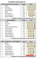
May 19, 2023--China Micro Semiconductor Equipment (Shanghai) Co., Ltd. (hereinafter referred to as "China Micro", SSE stock code: 688012) announced the 2023 customer conference held by TechInsights, a global technology analysis and intellectual property service provider Won six awards in the Satisfaction Survey (CSS), among which it ranked first in two lists of THE BEST Suppliers of Fab Equipment to Specialty Chip Makers and Deposition Equipment.
In addition to winning the highest evaluation from customers in the above two lists, AMEC also won the following four awards:

Ranked No. 3 among 10 BEST Focused Suppliers of Chip Making Equipment

Ranked No. 1 among THE BEST Suppliers of Fab Equipment to Specialty Chip Makers

Ranked third among global wafer manufacturing equipment suppliers (THE BEST Suppliers of Fab Equipment)

Ranked fifth among THE BEST Suppliers of Fab Equipment to Foundation Chip Makers
1684500861578.png
 

tokenanalyst

Brigadier
Registered Member
Zhichun Technology (PNCS) intends to invest in the construction of semiconductor electronic chemicals, electronic special gas research and development and industrialization projects in Shanghai

According to "PNC Zhichun Technology" news, on May 16, Zhichun Technology signed an investment intention agreement with Shanghai Chemical Industry Zone. Zhichun Technology intends to invest in the construction of semiconductor electronic chemicals, electronic special gas research and development and industrialization projects in the Shanghai Electronic Chemicals Zone.
It is understood that at the end of 2020, the Shanghai Chemical Industry Zone officially launched the construction of the "Shanghai Electronic Chemicals Zone", focusing on integrated circuit related products such as photoresists and supporting materials, electronic special gases, wet electronic chemicals and CMP polishing materials, and making every effort to create electronic products. Chemical research and development test base, production base and logistics storage base.
Jiang Yuan, chairman and general manager of Zhichun Technology, said electronic chemicals are of great significance to semiconductor manufacturing, especially advanced processes, including logic chips and memory chips. In the future, Zhichun Technology will continue to deeply cultivate the integrated circuit industry, provide trinity services around "craft-equipment-material", and build Chinese brands against top international companies.

Please, Log in or Register to view URLs content!
 

tokenanalyst

Brigadier
Registered Member

Dinglong shares: 14nm advanced technology STI process polishing pad project started​


On May 18, at the start-up site of major projects in Wuhan Economic Development Zone, Dinghui Microelectronics STI process polishing pad development and industrialization project, integrated circuit polishing process material intelligent upgrading and transformation project started intensively.

It is reported that the STI process polishing pad development and industrialization project mainly builds R&D laboratories and production workshops to form an annual production capacity of 200,000 pieces of 14nm advanced STI process polishing pads to meet the needs of the high-end market. The intelligent upgrading and transformation project of integrated circuit polishing process materials will purchase new equipment and configure intelligent systems to achieve deep system integration and improve the core competitiveness of products.

Dinghui Microelectronics is a CMP polishing supplier under Dinglong Holdings that masters the core R&D and manufacturing technology of the entire polishing pad process. In 2022, Dinglong will achieve revenue of 2.721 billion yuan, a year-on-year increase of 15.52%; net profit attributable to the parent company will be 390 million yuan, a year-on-year increase of 82.66%. It pointed out that the main reasons affecting the changes in the net profit of shareholders of listed companies are: the profit of the CMP polishing pad business in the new business sector has increased significantly with the increase in revenue, and the overall profit of the consumables sector has increased due to the increase in revenue, the increase in product gross profit and the impact of exchange rate changes. Profit increased significantly year-on-year.


Please, Log in or Register to view URLs content!
 

tokenanalyst

Brigadier
Registered Member

Domestic SiC substrate laser lift-off achieves a new breakthrough​


Recently, Chen Tong, chairman of Tyco Tianrun, said that the key to breaking through 1 million pieces of domestic SiC single projects is cost, that is, "the cost of silicon carbide devices is only twice that of silicon devices."

The cost reduction of silicon carbide devices requires the joint efforts of the entire industry chain. Among them, the cost of silicon carbide substrates accounts for about 50%, so new technologies are urgently needed to "cut down" the cost. There are two major bottlenecks in the cost reduction of silicon carbide substrates . In addition to crystal growth, there is also ingot cutting . At present, the mainstream cutting technologies for silicon carbide substrates include mortar wire cutting, diamond wire cutting, etc. However, the loss rate of traditional cutting technologies is too high and the working hours are too long.Taking mortar wire cutting as an example, as many as 40% of silicon carbide ingots are wasted in the form of dust, and the high-speed running process of the cutting wire will also cause 20~50μm rough undulations and surface/subsurface structure damage. According to analysis , The total material loss of silicon carbide multi-wire cutting technology is as high as 30%~50%. At the same time, it usually takes about 150 hours to cut a 6-inch SiC ingot, which is not conducive to the rapid delivery of SiC substrates. In addition, the Ra value of the substrate after dicing is relatively large, and three processes of rough grinding, fine grinding and CMP are required, which take more than 5 daysin total .
MBXY-CR-fa1a0ce04beb6a5ec344387819b2d3fa.png

If laser lift-off technology is used instead , it is expected to greatly reduce the cost of silicon carbide substrates. Laser lift-off technology is to form a modified layer inside the silicon carbide ingot through laser treatment, so that the wafer is peeled off from the silicon carbide ingot. This technology has the advantages of low material loss, high processing efficiency, and a large number of wafers, and the total material loss rate can be reduced to about 30%-50%(depending on the type of ingot).If the laser lift-off technology is successfully applied to the mass production of silicon carbide substrates , it will surely bring a new model of light assets and high benefits to the silicon carbide industry , which is expected to further reduce the cost of silicon carbide devices and promote the application of silicon carbide devices in a wider range of fields .
MBXY-CR-6cc69e9f957ce71146a05e5f95b7c90f.png

Foreign manufacturers in the silicon carbide industry have been exploring laser lift-off technology for more than five years . As of now, laser lift-off technology has not been introduced into mass production lines, and there are still some technical challenges to be resolved. According to "experts say three and a half generations", West Lake Instruments has achieved a breakthrough in the laser lift-off technology of silicon carbide substrates, and has successfully developed a complete set of laser lift-off equipment for silicon carbide substrates , which can be directly put into production , providing a solid foundation for the production of silicon carbide substrates new and efficient solutions.

If you want to learn more about Westlake Instruments' silicon carbide substrate laser lift-off technology, please sign up to participate in the "Automotive and Optical Storage SiC Application and Supply Chain Upgrade Conference" held in Shanghai on May 25. At that time, Westlake University National Qiang Chair Professor and Vice President Qiu Min, and West Lake Instruments CEO Liu Dongli will attend this meeting, among which Qiu Min will give a speech "Advanced Optoelectronic Technology, Helping Industrial Innovation" , and West Lake Instruments CEO Liu Dongli will release silicon carbide substrates at the meeting New product in laser stripping equipment.

Please, Log in or Register to view URLs content!
 

tphuang

Lieutenant General
Staff member
Super Moderator
VIP Professional
Registered Member

Dongxin: The company's advanced process 1xnm NAND Flash product has completed functional verification​


642721735678.4827.png


Jiwei.com News On May 17, Dongxin shares disclosed the latest research summary, saying that the company's SLC NAND Flash continued to develop new products on the 28nm and 24nm process, and continued to expand the SLC NAND Flash product line. During the reporting period, some new products have been released. Reach the mass production standard. The company's advanced 1xnm NAND Flash products have completed the first round of wafer tape-out and the first wafer manufacturing, and have completed functional verification.

At the same time, the company's NOR Flash products continue to develop new products with higher capacity on the 48nm process of PSMC. Currently, samples of 512Mb and 1Gb large-capacity NOR Flash products are available to customers. On the other hand, the company's NOR Flash product process in SMIC has advanced from 65nm to 55nm. At present, the process line has completed the first wafer tape-out. The LPDDR4x and PSRAM products designed and developed by the company have completed engineering samples and passed customer verification.

This is closely related to the fact that Dongxin Technology attaches great importance to and maintains a high level of R&D investment. In 2022, Dongxin's research and development expenses will be 110 million yuan, accounting for 9.63% of the current operating income, a year-on-year increase of 47.46%. As of the end of 2022, the company has a total of 130 R&D and technical personnel, an increase of 49.43% over the same period last year.

Dongxin shares stated that the company will maintain the technological advancement of the company's existing products through continuous R&D innovation, process upgrades and performance iterations. On the basis of the existing application fields, the company will increase the layout and development of emerging fields such as the Internet of Things, intelligent hardware applications, automotive electronics, and medical health, increase the market share of the company's products, and simultaneously increase the value of customized products and services. ability. The company will also adhere to the core of storage products, expand intelligent extension and be application-oriented, develop distinctive storage products, and increase profit margins through differentiation; continue to develop domestic high-quality customers, serve important customers in the industry, and gradually expand overseas markets. Enhance the company's global market position and influence.

Please, Log in or Register to view URLs content!

Questions about this
东芯股份披露最新调研纪要称,公司的SLC NAND Flash在28nm及24nm的制程上持续开发新产品,不断扩充 SLC NAND Flash 产品线,报告期内部分新产品已达到量产标准。公司先进制程的1xnm NAND Flash产品已完成首轮晶圆流片及首次晶圆制造,并已完成功能性验证。
SLC NAND Flash. are the nm here the same as logic process nm? How should we be thinking about the technical progression of SLD NAND?

同时,公司的 NOR Flash 产品在力积电的 48nm制程上持续进行更高容量的新产品开发,目前 512Mb、1Gb 大容量 NOR Flash 产品都已有样品可提供给客户。另一方面,公司在中芯国际的 NOR Flash 产品制程从 65nm 推进至 55nm,目前该制程产线已完成首次晶圆流片。而公司设计研发的 LPDDR4x 及 PSRAM 产品均已完成工程样片并已通过客户验证。

so in this one, powerchip produces their 48nm NOR Flash.
SMIC has progressed from 65nm to 55nm and just taped out the first wafer. That tells me SMIC is behind in NOR Flash products and just reached 55nm process. Sounds reasonable? Is 48nm the leading NOR Flash process?

关于公司在SLC NAND方面的优势,东芯股份表示,公司的 SLC NAND Flash凭借产品品类丰富、功耗低、可靠性高等特点,可以满足客户在不同应用领域及应用场景的需求。公司开发的 SLC NAND Flash 产品使用温度范围可达到-40℃~105℃,部分产品已经通过 AEC-Q100 的验证;凭借高可靠性,被广泛应用于通讯设备、安防监控、可穿戴设备及移动终端等领域,通过了联发科、瑞芯微、国科微、博通等行业内主流平台厂商的认证。
notice here the requirements of SLC NAND Flash to past AEC-Q100 (auto grade I think) and usage bw -40 to 105C.
Anyone knows where the domestic fabs are at with NAND Flash?

Looks like plenty of room for improvement on the "mature" process stuff.
 

tokenanalyst

Brigadier
Registered Member

tokenanalyst

Brigadier
Registered Member
Questions about this
Dongxin shares disclosed the latest survey minutes, saying that the company’s SLC NAND Flash continued to develop new products on the 28nm and 24nm processes, and continued to expand the SLC NAND Flash product line. During the reporting period, some new products have reached mass production standards. The company's advanced 1xnm NAND Flash products have completed the first round of wafer tape-out and first wafer manufacturing, and have completed functional verification.
SLC NAND Flash. are the nm here the same as logic process nm? How should we be thinking about the technical progression of SLD NAND?

At the same time, the company's NOR Flash products continue to develop new products with higher capacity on the 48nm process of PSMC. Currently, samples of 512Mb and 1Gb large-capacity NOR Flash products are available to customers. On the other hand, the company's NOR Flash product process in SMIC has advanced from 65nm to 55nm. At present, the process line has completed the first wafer tape-out. The LPDDR4x and PSRAM products designed and developed by the company have completed engineering samples and passed customer verification.

so in this one, powerchip produces their 48nm NOR Flash.
SMIC has progressed from 65nm to 55nm and just taped out the first wafer. That tells me SMIC is behind in NOR Flash products and just reached 55nm process. Sounds reasonable? Is 48nm the leading NOR Flash process?

Regarding the company's advantages in SLC NAND, Dongxin said that the company's SLC NAND Flash can meet the needs of customers in different application fields and application scenarios by virtue of its rich product categories, low power consumption, and high reliability. The temperature range of SLC NAND Flash products developed by the company can reach -40℃~105℃, and some products have passed the verification of AEC-Q100; with high reliability, they are widely used in communication equipment, security monitoring, wearable devices and mobile terminals In other fields, it has passed the certification of mainstream platform manufacturers in the industry such as MediaTek, Rockchip, Goke Micro, and Broadcom.
notice here the requirements of SLC NAND Flash to past AEC-Q100 (auto grade I think) and usage bw -40 to 105C.
Anyone knows where the domestic fabs are at with NAND Flash?

Looks like plenty of room for improvement on the "mature" process stuff.
Looks like that NAND flash has its own lithography process with its own issues and caviats.

Flash Memory Construction​

A single bit of flash memory is constructed of a transistor with a floating gate. The floating gate can be used to store electrons for an extended time. Electrons get to the floating gate by tunneling through to the thin oxide layer that isolates the floating gate (Figure 2). This tunneling effect is created when a large gate voltage is applied to the device. The gate voltage creates a field in the channel, increasing the energy of the electrons and causing some of them to tunnel through the thin oxide layer. The charge can be removed from the floating gate by reversing the gate voltage and pushing the electrons back through the thin oxide layer.

Please, Log in or Register to view URLs content!
Figure 2: Storage via floating gate.
When electrons are stored on the floating gate, the threshold voltage, or the gate voltage where the transistor begins to conduct, changes. If there are no electrons on the gate, then the transistor acts like a normal MOSFET. When electrons are stored on the floating gate, their negative charge shields the conductive channel from the gate and prevents or limits the current flow from the source to the drain. This change in the threshold voltage modulates the current/voltage characteristics of the cell, so the status of the floating gate can be read by simply applying a voltage to the terminals and measuring the resulting current.
Please, Log in or Register to view URLs content!


As the NAND flash lithography nodes are scaled down, the number of electrons available to move to the floating gate decreases. This is a well discussed fact for MLC NAND, but the same physics applies directly to SLC flash as well. In smaller lithographies, a small change in the number of electrons on the floating gate can dramatically affect the threshold voltage (Figure 3). With each reduction in NAND flash lithography, it becomes very difficult to achieve the same performance and endurance of the previous process node. The reduced number of electrons available makes smaller lithography devices even more susceptible to threshold voltage shifts caused by damage, leakage or disruptions.

Please, Log in or Register to view URLs content!
Figure 3: Any change in charge will affect the threshold voltage of a cell.
The gate threshold voltage is variable regardless of what lithography a NAND cell is made on. As it can be affected by a number of factors, it is typically expressed as a statistical distribution. The statistical distribution of the threshold voltage on new flash defines the difference between a programmed and an erased cell. The voltages used in programing a NAND flash cell slowly damage the thin oxide layer that isolates the floating gate, allowing more charge to be trapped on the floating gate. At any geometry, this damage will accumulate over time, narrowing the gap between the threshold regions and pushing the threshold voltage of an erased cell over the detection threshold used to detect the programmed state (Figures 4, 5). At smaller lithographies the geometries used in the NAND construction are even smaller, resulting in faster wear out and lower endurance. In an embedded system this means that the same software application can wear out newer SLC NAND at much faster rates than ever before.

Please, Log in or Register to view URLs content!
 
Status
Not open for further replies.
Top