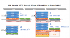
Dr. Hong Qiyuan ICMO Technology Co., Ltd. introduced the company's three-dimensional heterogeneous integration technology: HITOC, which is actually two technical routes of Wafer on wafer and Die on wafer. Wafer on wafer can be of the same type, different types, or even different process nodes. Take the logic + DRAM that we have produced tens of thousands of pieces as an example. We connect the logic wafer and DRAM wafer together through Hybrid Bonding, and then lead them out through thinning, through-silicon vias, and metal wires, and then cut and package them. It becomes a Chip with no difference in a single chip. Another technical route is Die on Wafer, which is achieved by putting the cut EU tape, which is also Hybrid Bonding, on the Wafer, and then through injection molding, thinning, silicon perforation, metal wire lead-out and other processes. In addition to the one-on-one-on-wafer solution, our Wafer on wafer can also do multi-wafer stacking. Currently, we have achieved five wafers, that is, four DRAMs plus one SOC. We have already achieved this 4+1 technology. Ready, and this kind of sample is being tested, the process flow of Die on wafer has also been well established, and it is now doing the test. In addition, our three-dimensional heterogeneous integration also includes the technical form of Die on wafer. There are four types. The first is a typical 2.5D package. Our Memory and SOC are connected together. Customers only need to focus on the SOC The design is just fine. The one on the right is the real 3D package. The difference is that the connection is replaced by Hybrid Bonding, which can provide millions of connections, and improve the bandwidth and connection density to the highest extent. The third is the real 3D IC, which uses 1+4 stacking technology to realize the real integration of memory and logic. The fourth is the extension of 1 to 3. In addition to technologies such as Die on wafer and 1+4, we can usually put some slow logic, IO, power management and other chips into it. The SOC only needs to concentrate on making The part it does best is just fine.

He also mentioned that 3D heterogeneous integration involves software, hardware, design, process, interface, etc., how to disassemble a chip, and what process is most suitable for each module. In fact, the threshold is quite high. Between DRAMs, each IP is required to be neutral, so this industry needs a fully capable and neutral heterogeneous integration support platform. With more participants working together to formulate standards, the ecology can be improved, and the chip industry can have no difficult heterogeneous integration.
High-performance packaging boosts the development of heterogeneous integration
Zheng Li, CEO of Jiangsu Changdian Technology Co., Ltd., believes that high-performance computing has led the industry to Chiplet and high-performance computing. Here, I would like to remind everyone that heterogeneity is not only the more common memory chips and computing power chips. In fact, when we talk about 2.5D and 3D packaging, we pay more attention to the need for integration in heterogeneity. To, for example, sensors, power devices, and even optical devices, the structure of heterogeneous heterogeneous chiplets assembled together. But this is just a path for heterogeneous integration or high-performance packaging
SiP has developed to this day, and system integration has formed higher-density, higher-bandwidth connections. From an international academic point of view, such a path is also regarded as an important path for heterogeneous heterogeneous high-performance packaging, but we One difference from 2.5D and 3D packaging is that 2.5D and 3D are based on wafer-level packaging technology, which has a higher standard in terms of bandwidth and connection. But it also has some limitations in terms of heterogeneity.
We believe that whether it is 2.5D, 3D packaging, or high-density SiP packaging, it is an important path for the development of high-performance packaging.
It is true that our circuits were originally developed with the integration of transistors as the core. Today's technology applications push us to take the system as the core and the system architecture as the core to continue to promote integrated circuits, not just reliability, or some physical Performance, but the performance of the entire integrated circuit product, its performance must be developed forward. Therefore, we say that the integration technology of the integrated circuit driven by the system with the chiplet architecture or the high-performance SiP architecture as the core will continue to promote the development of our integrated circuits.
There are many new challenges for the design industry, manufacturing industry, and packaging and testing industry. Product design engineers must have a deeper understanding of the design of the entire microsystem and have stronger design capabilities. The diversification of packaging methods, from the design of TSV, Interposer, etc. to wiring, requires packaging and testing manufacturers to cooperate with upstream and realize it with higher-precision automated equipment production lines.
When referring to CPI, we often say that Packag fulfills the requirements for reliability and realizes it through CPI. Today, because of the high-performance packaging, CPI itself, and the interaction between Packag, it has played a decisive role in the chip product itself. This is about the design collaboration CPI between the fab and the packaging factory. From the point of view of design and packaging, as I mentioned just now, such collaborative design, from the initial architecture design of the product, the product design engineer must closely cooperate with the enterprise responsible for the subsequent manufacturing of the microsystem integration. This is also a pleasure. It can encapsulate the changes in the links between the industrial chains brought to us.
The core feature of high-performance packaging is that it must be based on high-bandwidth, high-density integration. Encapsulation is not only a process of encapsulation and packaging, but more importantly, a process of cascading and connecting. The advent of high-performance packaging has made design, packaging, and manufacturing inseparable. The emergence of a new design and development path is STCO. The tools and methods used in the development of this product must be developed from the perspective of the system, combined with manufacturing technology and production technology. This is also a One of the important features.
Intelligent application scenarios generate high-performance computing and storage requirements, and high-demand drives the development of chip technology. High-performance packaging such as SiP packaging, photoelectric packaging, 2.5D\3D packaging, and small chips will become the basic configuration in the future. . We call for the entire industrial chain, especially the equipment and material industry chain, to develop towards a high degree of automation and high-precision materials.

