Chinese semiconductor industry

Status
Not open for further replies.

tphuang

Lieutenant General
Staff member
Super Moderator
VIP Professional
Registered Member
listening to Huawei Ascend conference from earlier this month talking about their 鹏城云脑 program
Please, Log in or Register to view URLs content!

Please, Log in or Register to view URLs content!
根据《人工智能计算中心发展白皮书2.0》,鹏城云脑Ⅱ主设备Atlas900AI集群,由4096颗昇腾910AI处理器构成,算力达E级,荣获AIPerf(大规模人工智能基准评测程序)榜单第一名,并保持IO500(高性能计算存储系统性能排行榜-全系统输入输出和10节点系统)两项世界记录,其中在全系统输入输出性能得分是排名第二得分的近20倍,为盘古大模型等国产头部AI大模型训练提供了坚实、先进的基础算力底座。
according to this. PengchengII uses Atlas900 AI cluster w/ 4096 Ascend 910 GPU (and 2048 kunPeng-920 CPU)

It won AIPerf competition in China several years in a row now (most recently about 6 months ago)
Please, Log in or Register to view URLs content!
“鹏城云脑II”是鹏城实验室联合国内优势科研力量,在深圳市大力支持下打造的人工智能大科学装置,用于AI领域诸如计算机视觉、自然语言处理、自动驾驶、智慧交通、智慧医疗等各类基础性研究与探索。“鹏城云脑II” 包括4096颗昇腾910 AI处理器和2048颗鲲鹏920 CPU处理器,可以提供1E OPS智能算力,即不低于每秒100亿亿次操作的AI计算能力,截止目前已累计运行超过600天。
with 4096 Ascend 910, it can provide 1 ExaFlops of computation. Looks like this is with earlier 256 TFLOPS Ascend 910, rather than the recent 320 TFLOPS Ascend 910. And it has been used now over 600 days for ADAS, natural language processing, ADAS, Smart transportation, smart medicine and other research

Please, Log in or Register to view URLs content!
What a lot of people don't appreciate and that video mentioned is that the original Baidu Erniebot was trained in the Pengcheng lab in Shenzhen
文言一心来自深圳百度的鹏城云脑二期项目,可以挖掘参与鹏城云脑项目的建设方,如深圳本土一线国资特发集团下的上市公司
Please, Log in or Register to view URLs content!
,过年两年曾中标28亿订单该项目。

Now you wonder why I'm wasting time with this well the most important part of that video is probably this part
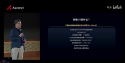
Screen Shot 2023-05-19 at 2.14.15 PM.png

They are planning a Pengcheng YunNao III project (鹏城云脑III)
will use their own GPU/NPU product & ecosystem
16 EFLOPS @ FP16
expect to be top in the world in I/O (10500)
top the world in AI training
will provide for 6G loud lab
will provide training for large model
hoping to have ready by end of the year

this is 16x YunNao II (which was 1 EFLOP, remember the 4096 x256 TFLOPS of earlier Ascend 910 GPU)

If you listen to the 8 minute mark of this clip, he said, it will use Huawei's new GPU/NPU. So this confirms that Ascend-920 & Kunpeng-930 will be ready by the end of this year.

That will be a huge. And the YunNao III lab will be as large as GPT 4.0 probably, in the same ballpark and 4x that of Baidu's large data center
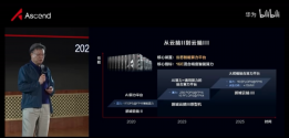
Screen Shot 2023-05-19 at 2.20.59 PM.png
Again, this just confirms they are aiming to have prototype of it starting computation this year and have it fully built by 2025. Pengcheng 2 was ready with 1 EFLOP by 2020. Will be built around Shenzhen.
 

hvpc

Junior Member
Registered Member
Questions about this
东芯股份披露最新调研纪要称,公司的SLC NAND Flash在28nm及24nm的制程上持续开发新产品,不断扩充 SLC NAND Flash 产品线,报告期内部分新产品已达到量产标准。公司先进制程的1xnm NAND Flash产品已完成首轮晶圆流片及首次晶圆制造,并已完成功能性验证。
SLC NAND Flash. are the nm here the same as logic process nm? How should we be thinking about the technical ásprogression of SLD NAND?
this is planar NAND Flash, precursor to 3D NAND. for most fabs, 1x nm NAND (18/19nm) is probably the limit. for higher density, it’d make more sense to move to 3D-NAND instead of pursuing 16nm or even 14nm planar NAND. The resolution required for 16nm and 14nm wouldn't be worth the trouble.

同时,公司的 NOR Flash 产品在力积电的 48nm制程上持续进行更高容量的新产品开发,目前 512Mb、1Gb 大容量 NOR Flash 产品都已有样品可提供给客户。另一方面,公司在中芯国际的 NOR Flash 产品制程从 65nm 推进至 55nm,目前该制程产线已完成首次晶圆流片。而公司设计研发的 LPDDR4x 及 PSRAM 产品均已完成工程样片并已通过客户验证。


so in this one, powerchip produces their 48nm NOR Flash.
SMIC has progressed from 65nm to 55nm and just taped out the first wafer. That tells me SMIC is behind in NOR Flash products and just reached 55nm process. Sounds reasonable? Is 48nm the leading NOR Flash process?
The “leading edge” NOR node is 45nm NOR. this is the NOR barrier, the leading edge has been at 45nm for at least a decade now.

关于公司在SLC NAND方面的优势,东芯股份表示,公司的 SLC NAND Flash凭借产品品类丰富、功耗低、可靠性高等特点,可以满足客户在不同应用领域及应用场景的需求。公司开发的 SLC NAND Flash 产品使用温度范围可达到-40℃~105℃,部分产品已经通过 AEC-Q100 的验证;凭借高可靠性aaaa,被广泛应用于通讯设备、安防监控、可穿戴设备及移动终端等领域,通过了联发科、瑞芯微、国科微、博通等行业内主流平台厂商的认证。
notice here the requirements of SLC NAND Flash to past AEC-Q100 (auto grade I think) and usage bw -40 to 105C.
Anyone knows where the domestic fabs are at with NAND Flash?
XMC still makes planar NAND. They should at least have 5xnm NAND
 

antiterror13

Brigadier
I think they are trying to be closer to their market, ASML could offer higher bonuses to snap talent from their competition, also by building China specific solutions could entice Chinese costumers to buy from them risk free solutions instead of the competition. The more you have the more you get.

This news also tell me that ASML is confident that the big bully won't be successful in trying to stop selling lithography to China
 

tphuang

Lieutenant General
Staff member
Super Moderator
VIP Professional
Registered Member
this is planar NAND Flash, precursor to 3D NAND. for most fabs, 1x nm NAND (18/19nm) is probably the limit. for higher density, it’d make more sense to move to 3D-NAND instead of pursuing 16nm or even 14nm planar NAND. The resolution required for 16nm and 14nm wouldn't be worth the trouble.
With 3D NAND so popular, where does planar NAND flash still get used?

If 1x is the limit, then why is XMC making 5xnm? What kind of device would use something that slow?
The “leading edge” NOR node is 45nm NOR. this is the NOR barrier, the leading edge has been at 45nm for at least a decade now.
Interesting, so SMIC has had a decade and is still 1 or 2 level behind that leading edge? Are they just not focused on it? It seems like all these fabs are talking about NOR flash, so there are clearly plenty of demand for it.
 

hvpc

Junior Member
Registered Member
With 3D NAND so popular, where does planar NAND flash still get used?

If 1x is the limit, then why is XMC making 5xnm? What kind of device would use something that slow?

Interesting, so SMIC has had a decade and is still 1 or 2 level behind that leading edge? Are they just not focused on it? It seems like all these fabs are talking about NOR flash, so there are clearly plenty of demand for it.
There are still some lower capacity NAND Flash use cases where SLC NAND come into play. also some industrial and auto use cases require consistency where same product once qualified is used over a long time, e.g. decade

XMC makes 5x nm NOR. Limit of NOR is 45nm, XMC is near the leading edge of NOR. NOR and NAND are not the same, can’t compare them through the “nm” node convention. NOR is known to have faster READ time, but slow WRITE time, so widely used in automotive. Most functions in our car, the program is loaded once and rarely updated, and yet we READ or uses the program often on daily basis. So the behavior of NOR makes it a good fit

NOR is niche market that Winbind had thrived in while other memory guys chose to stop fabbing it. There’s not as much money there so only a handful of people make it. China in its quest to gain presence in semi are looking for low hanging fruits. So looks like chinese fab are getting into this small niche market to compete with Winbind, MXIC, XMC.

for SLC NAND for auto, it wont be easy to take business from existing players. Once product is qualified, automotive company do not go around finding second vendor. Like I said earlier, they stick with same product for a long time. Any SLC NAND business new fab goes after would be new business opportunities
 

ZeEa5KPul

Colonel
Registered Member
for SLC NAND for auto, it wont be easy to take business from existing players. Once product is qualified, automotive company do not go around finding second vendor.
That's how it works in a normal market. China is not a normal market for two reasons: primarily, present US sanctions and the threat of future ones. Secondarily, Chinese industrial policy. Once suppliers are ready, regulators can mandate purchase quotas for Chinese chips on automobile companies operating in China.
 

Wahid145

Junior Member
Registered Member
And by the way tungsten deposition (W-CVD) is one of the technologies that the stooges think tankers were talking about in their big brain presentation in Washington D.C. to the Chicken-Hawk politicians before the ban on YMTC where they discussed equipment-materials for the production of semiconductor devices and obviously in a demonstration of knowledge of the industry they mostly talked about deposition equipment as if it were the only equipment used in a semiconductor factory, well, they ended up telling the politicians in D.C. that it was necessary to introduce export controls because China did not have this type of equipment, it seems that it did not age well.
Do you have a link to this? I'm really curious as to what they were saying.
Also, what kind of CVD/PVD is required for 7nm logic chip? There are so many CVD in AMAT website, being a newbie in this field I'm not sure which of those CVD and Etching products are required for sub 10 nm Logic Chip (for example, as you mentioned, WCVD is required for advanced DRAM)
 

FairAndUnbiased

Brigadier
Registered Member
Do you have a link to this? I'm really curious as to what they were saying.
Also, what kind of CVD/PVD is required for 7nm logic chip? There are so many CVD in AMAT website, being a newbie in this field I'm not sure which of those CVD and Etching products are required for sub 10 nm Logic Chip (for example, as you mentioned, WCVD is required for advanced DRAM)
There's actually been alot of innovation in mature nodes independent of lithography and die shrinks.

For example, CVD HfO2 gate dielectric was introduced at the 65 nm node while previously they used in situ oxidation to form SiO2 gate dielectric. And there's the previous case of W gate metal.

However its not that simple because you need both good adhesion and suppression of chemical diffusion between the channel, gate dielectric and gate metal. Otherwise, you get either mechanical instability (delamination) during further processing, or device failures due to phenomena such as unexpected conductivity, caused by point defects in gate dielectrics creating defect states in the bandgap. And there are also things that only manifest over a long time, like electromigration, yet still reduce device performance/lifetime.

That's why you also need things like Ti deposition, to form diffusion barriers. So you're having deposition and etch processes specifically for not only functional components (gate dielectric, gate metal) but also the diffusion barriers between each, etchstop layers, etc. You need Co-W to interface between W and Cu interconnect, TaN as a diffusion barrier between Cu and low-k dielectric, etc.

As you can see, for complicated logic chips there are many deposition chambers each carrying out complicated gas phase chemical reactions occuring in high aspect ratio spaces. For 3D NAND, you also need high aspect ratio etching.
 

GiantPanda

Junior Member
Registered Member
There are still some lower capacity NAND Flash use cases where SLC NAND come into play. also some industrial and auto use cases require consistency where same product once qualified is used over a long time, e.g. decade

XMC makes 5x nm NOR. Limit of NOR is 45nm, XMC is near the leading edge of NOR. NOR and NAND are not the same, can’t compare them through the “nm” node convention. NOR is known to have faster READ time, but slow WRITE time, so widely used in automotive. Most functions in our car, the program is loaded once and rarely updated, and yet we READ or uses the program often on daily basis. So the behavior of NOR makes it a good fit

NOR is niche market that Winbind had thrived in while other memory guys chose to stop fabbing it. There’s not as much money there so only a handful of people make it. China in its quest to gain presence in semi are looking for low hanging fruits. So looks like chinese fab are getting into this small niche market to compete with Winbind, MXIC, XMC.

for SLC NAND for auto, it wont be easy to take business from existing players. Once product is qualified, automotive company do not go around finding second vendor. Like I said earlier, they stick with same product for a long time. Any SLC NAND business new fab goes after would be new business opportunities

You cannot stick with a product that can be banned by a foreign power that already has a record of banning chips targeted at your country. Any CEO that doesn't look at a domestic alternative in this case is suicidal.
 

tphuang

Lieutenant General
Staff member
Super Moderator
VIP Professional
Registered Member
Please, Log in or Register to view URLs content!
Huawei Hisilicon V811 chip has been unveiled 4K display

Don't have the nm process or anything like that. But in this day & age, SMIC growth is tied to Huawei growth in some ways, since Huawei just can't make its own advanced chips in the near future. As Huawei & Hisilicon grab back more of its market share in different space, SMIC will gain market share also

Actually, looks like it's an improved version of 鸿鹄818 https://baike.baidu.com/item/鸿鹄818/23665699
which is made up of A73+A53双架构4核CPU和4核G51 GPU

So looks like this is actually going to require at least FinFET process.
 
Last edited:
Status
Not open for further replies.
Top