You are using an out of date browser. It may not display this or other websites correctly.
You should upgrade or use an alternative browser.
You should upgrade or use an alternative browser.
Chinese semiconductor industry
- Thread starter Hendrik_2000
- Start date
- Status
- Not open for further replies.
Saw in internet. Not sure you posted before. @tokenanalyst
Patent name: A laser plasma type extreme ultraviolet (LPP-EUV) lithography machine light source system
Application date 2022 .06 .23 Applicant Aerospace Information Innovation Institute, Chinese Academy of Sciences
The disclosure provides a laser plasma type extreme ultraviolet lithography machine light source system, the light source system is relatively miniaturized so that the EUV lithography machine has the advantages of compactness and small size, which is suitable for mass production and supply to the market, and further replacement of gadolinium targets occurs Detectors or other targets can generate EUV light with a wavelength of 6.7nm or shorter.
ASML's existing EUV lithography machine is a very large device. Also due to factors such as its bulky size, complex devices, high cost, and poor flexibility, its application has been limited, and it has become a "stuck neck" problem in my country's high-end chip industry. In addition, it is difficult for the ASML scheme to further increase the laser pulse power and pulse energy, which makes it difficult to develop LPP‑EUV for other more promising elements, such as gadolinium plasma at a radiation wavelength of 6.7nm.
专利名:一种激光等离子体型极紫外(LPP-EUV)光刻机光源系统
申请日 2022 .06 .23 申请人 中国科学院空天信息创新研究院
本公开提供的一种激光等离子体型极紫外光刻机光源系统,该光源系统相对小型化使得EUV光刻机具有紧凑、小型的优点,适于大批量生产供应市场,进一步换用钆靶材发生器或其他靶材可产生波长为6.7nm或更短波长的EUV光。
ASML公司现有的EUV光刻机是一种超大型装置。同样由于其体积庞大、装置复杂、造价成本昂贵、灵活性差等因素限制了它的应用,目前已成为我国高端芯片产业一个“卡脖子”问题。此外,ASML方案想要进一步提高激光脉冲功率和脉冲能量很困难,这使得研发其他更有前途的元素的LPP‑EUV存在困难,如钆等离子体在6 .7nm的辐射波长。
一种高重复频率的极紫外辐射光源及EUV光刻机光源
中国科学技术大学 申请日 2022 .06 .30
本发明提供了一种高重复频率的极紫外辐射光源及EUV光刻机光源
一种高功率EUV光刻光源的双脉冲驱动光源
中国科学院上海光学精密机械研究所 申请日 2022 .11 .16
本发明提供一种高功率EUV光刻光源的双脉冲驱动光源,旨在利用掺Tm全固态激
光器的波长在EUV激发效率上与CO2激光器相当,并且Tm离子上能级寿命长等特性,实现高
平均功率、高插墙效率的驱动光源,获得相比目前CO2驱动光源更经济且更高功率的解决方
案,获得高功率EUV辐射输出,解决EUV光刻机芯片产量提升的问题
Since ASML EUV with 13.5nm wave length can produce 7nm chips can this produce 3nm chips? , My knowledge is basic at best in this field btwSaw in internet. Not sure you posted before. @tokenanalyst
Patent name: A laser plasma type extreme ultraviolet (LPP-EUV) lithography machine light source system
Application date 2022 .06 .23 Applicant Aerospace Information Innovation Institute, Chinese Academy of Sciences
The disclosure provides a laser plasma type extreme ultraviolet lithography machine light source system, the light source system is relatively miniaturized so that the EUV lithography machine has the advantages of compactness and small size, which is suitable for mass production and supply to the market, and further replacement of gadolinium targets occurs Detectors or other targets can generate EUV light with a wavelength of 6.7nm or shorter.
ASML's existing EUV lithography machine is a very large device. Also due to factors such as its bulky size, complex devices, high cost, and poor flexibility, its application has been limited, and it has become a "stuck neck" problem in my country's high-end chip industry. In addition, it is difficult for the ASML scheme to further increase the laser pulse power and pulse energy, which makes it difficult to develop LPP‑EUV for other more promising elements, such as gadolinium plasma at a radiation wavelength of 6.7nm.
专利名:一种激光等离子体型极紫外(LPP-EUV)光刻机光源系统
申请日 2022 .06 .23 申请人 中国科学院空天信息创新研究院
本公开提供的一种激光等离子体型极紫外光刻机光源系统,该光源系统相对小型化使得EUV光刻机具有紧凑、小型的优点,适于大批量生产供应市场,进一步换用钆靶材发生器或其他靶材可产生波长为6.7nm或更短波长的EUV光。
ASML公司现有的EUV光刻机是一种超大型装置。同样由于其体积庞大、装置复杂、造价成本昂贵、灵活性差等因素限制了它的应用,目前已成为我国高端芯片产业一个“卡脖子”问题。此外,ASML方案想要进一步提高激光脉冲功率和脉冲能量很困难,这使得研发其他更有前途的元素的LPP‑EUV存在困难,如钆等离子体在6 .7nm的辐射波长。
一种高重复频率的极紫外辐射光源及EUV光刻机光源
中国科学技术大学 申请日 2022 .06 .30
本发明提供了一种高重复频率的极紫外辐射光源及EUV光刻机光源
一种高功率EUV光刻光源的双脉冲驱动光源
中国科学院上海光学精密机械研究所 申请日 2022 .11 .16
本发明提供一种高功率EUV光刻光源的双脉冲驱动光源,旨在利用掺Tm全固态激
光器的波长在EUV激发效率上与CO2激光器相当,并且Tm离子上能级寿命长等特性,实现高
平均功率、高插墙效率的驱动光源,获得相比目前CO2驱动光源更经济且更高功率的解决方
案,获得高功率EUV辐射输出,解决EUV光刻机芯片产量提升的问题
saw another article about it hereZhongwei Company launched a 12-inch thin film deposition equipment!
Recently, AMEC Semiconductor Equipment (Shanghai) Co., Ltd. (hereinafter referred to as "AMEC", Shanghai Stock Exchange Stock Code: 688012) launched the self-developed 12-inch low-pressure chemical vapor deposition (LPCVD) equipment Preforma Uniflex™ CW. This is a new breakthrough made by China Microelectronics in the field of semiconductor thin film deposition, which has been deeply involved in high-end micro-processing equipment for many years, and it is also a new momentum to realize the diversified growth of the company's business.
As a 12-inch LPCVD equipment with high output efficiency and excellent performance independently developed by AMEC, Preforma Uniflex™ CW can flexibly configure up to five double reaction chambers (ten reaction chambers), and each reaction chamber can process simultaneously Two wafers, while ensuring lower production costs and chemical consumption, achieve higher production efficiency.
Preforma Uniflex™ CW, as an LPCVD equipment independently developed by AMEC, is equipped with an optimized gas mixing solution and heating stage with completely independent intellectual property rights. It has excellent film uniformity, filling ability and process adjustment flexibility. Large wafers, it also has good process capabilities. And its excellent step coverage and filling ability can meet the application requirements of filling contact holes and metal tungsten lines in advanced logic devices, DRAM and 3D NAND.
The Preforma Uniflex™ CW launched by AMEC is another milestone in the company's road to innovation. "This LPCVD equipment not only has complete and independent intellectual property rights, but also created a new record for the speed of research and development of new equipment in China Microelectronics." Said Tao Heng, Vice President of China Microelectronics Group, General Manager of LPCVD Product Department and Public Platform Engineering Department: "Since the establishment of this LPCVD equipment research and development project, we have completed product design, production prototype development and laboratory evaluation in less than half a year, and have successfully imported it to the client for production line approval."
View attachment 112365
very similar in content
this to me is the interesting part
They are going after the whole marketmetal tungsten lines in advanced logic devices, DRAM and 3D NAND.
if we go back to that FT article on CXMT
I wonder if AMEC is spreading news about its new product now because it's working closely with CXMT.“CXMT has set a very ambitious expansion target this year, even despite the memory chip downturn,” said one person with knowledge of the situation, adding that its annual capital expenditure would increase by about $4bn in 2023 as it boosted purchases of chipmaking equipment.
“CXMT plans to turn to more Chinese equipment suppliers for the expansion, so the capital expenditure can be raised by $5bn or even more. Testing the relatively immature domestic equipment requires additional cash,” said another person familiar with the situation.
And I also wonder if CXMT is trying out a de-americanized production line for 21 or 19nm process
Bro COMPARABLE with ASML HIGH NA EUVL? if YES then in 2025, when the rumored release of Chinese EUVL (LPP) then it had leveled with the collective west (ASML) and may surpass it with the operational of Beijing SSMB in 2026.Application date 2022 .06 .23 Applicant Aerospace Information Innovation Institute, Chinese Academy of Sciences
The disclosure provides a laser plasma type extreme ultraviolet lithography machine light source system, the light source system is relatively miniaturized so that the EUV lithography machine has the advantages of compactness and small size, which is suitable for mass production and supply to the market, and further replacement of gadolinium targets occurs Detectors or other targets can generate EUV light with a wavelength of 6.7nm or shorter.
by on May 26, 2022 10:00 AM EST
It took the semiconductor industry over a decade to prep everything needed for production of chips using extreme ultraviolet (EUV) lithography. It looks like it is going to take a lot less to reach the next level — EUV with High-NA.
Higher Resolution Needed
Nowadays the most advanced chips are made on 5/4-nm-class process using EUV lithography ASML's Twinscan NXE:3400C (and similar) systems that feature a 0.33 numerical aperture (NA) optics, which provides a 13 nm resolution. This resolution is good enough for a single-pattern approach at 7 nm/6 nm nodes with 36 nm ~ 38 nm pitches and at 5nm with 30 nm ~ 32 nm pitches. But as pitches get below 30 nm (at beyond 5 nm nodes) the 13 nm resolution might call for dual lithographic exposure that is going to be used for years to come.Huahong announcing Q1 earnings. Not great, as one might imagine. Just $630 million revenue with 32% margin. For Q2, also projecting $630 million revenue but with just 25 to 27% margin. They are expecting to slowly reach 95k wpm at Wuxi this year
Originally, they said they would do this by Q2, but looks like they have slowed things down a little bit due to weak demand
Originally, they said they would do this by Q2, but looks like they have slowed things down a little bit due to weak demand
I believe this is for Wuxi Fab 2并将适时启动新产线的建设,为公司特色工艺的中长期发展提供产能支持。
@tphuang, you are too tough on them. They are getting good gross margin of 32% and net profit of 22.3% and operating at >103% of wafer capacity. They have highest utilization in the foundry segment and more profitable than SMIC. Considering the market condition, I think this is good performance.Huahong announcing Q1 earnings. Not great, as one might imagine. Just $630 million revenue with 32% margin. For Q2, also projecting $630 million revenue but with just 25 to 27% margin. They are expecting to slowly reach 95k wpm at Wuxi this year
This is the expansion is for HuaHong Fab7 in Wuxi. This should be for the first fab in Wuxi, not the second fab. Fab7 currently at 65K wpm and merely competing the original plan ramp to 95K wpm.Originally, they said they would do this by Q2, but looks like they have slowed things down a little bit due to weak demand
I believe this is for Wuxi Fab 2
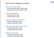
For more detailed info on Huahong’s 1Q23 result, this is the actual presentation material directly from HuaHong:
Last edited:
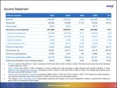
SMIC also released their 1Q23 result earlier today:
The lower revenue and the 20% gross margin was inline with SMIC’s guidance. The operating Margin ended up around 6% due to higher depreciation cost.
One thing I was surprised is the 15% Q/Q decrease in R&D expenses due to “lower level of R&D activities in 1Q23”. Hope this is just a temporary decrease in R&D activity.
the capacity utilization dropped to 68% in 1Q23.


Breakthrough 30% for the first time! ! The large-area efficiency of Yaoyang perovskite stacks leads the world.
The efficiency of the 25cm² large-area perovskite/crystalline silicon two-electrode stack cell made by Yao Energy Technology has made another breakthrough . It has been certified by the China Institute of Metrology, and the steady-state conversion efficiency of the cell has reached 30.83% , which is higher than that certified in February this year. The 29.57% of the battery has increased by 1.26%. It has once again refreshed the highest certification record for the efficiency of large-area laminated cells. It is the first to enter the era of 30%+, which is a milestone!- Status
- Not open for further replies.


