Link?Saw in internet. Not sure you posted before. @tokenanalyst
Patent name: A laser plasma type extreme ultraviolet (LPP-EUV) lithography machine light source system
Application date 2022 .06 .23 Applicant Aerospace Information Innovation Institute, Chinese Academy of Sciences
The disclosure provides a laser plasma type extreme ultraviolet lithography machine light source system, the light source system is relatively miniaturized so that the EUV lithography machine has the advantages of compactness and small size, which is suitable for mass production and supply to the market, and further replacement of gadolinium targets occurs Detectors or other targets can generate EUV light with a wavelength of 6.7nm or shorter.
ASML's existing EUV lithography machine is a very large device. Also due to factors such as its bulky size, complex devices, high cost, and poor flexibility, its application has been limited, and it has become a "stuck neck" problem in my country's high-end chip industry. In addition, it is difficult for the ASML scheme to further increase the laser pulse power and pulse energy, which makes it difficult to develop LPP‑EUV for other more promising elements, such as gadolinium plasma at a radiation wavelength of 6.7nm.
专利名:一种激光等离子体型极紫外(LPP-EUV)光刻机光源系统
申请日 2022 .06 .23 申请人 中国科学院空天信息创新研究院
本公开提供的一种激光等离子体型极紫外光刻机光源系统,该光源系统相对小型化使得EUV光刻机具有紧凑、小型的优点,适于大批量生产供应市场,进一步换用钆靶材发生器或其他靶材可产生波长为6.7nm或更短波长的EUV光。
ASML公司现有的EUV光刻机是一种超大型装置。同样由于其体积庞大、装置复杂、造价成本昂贵、灵活性差等因素限制了它的应用,目前已成为我国高端芯片产业一个“卡脖子”问题。此外,ASML方案想要进一步提高激光脉冲功率和脉冲能量很困难,这使得研发其他更有前途的元素的LPP‑EUV存在困难,如钆等离子体在6 .7nm的辐射波长。
一种高重复频率的极紫外辐射光源及EUV光刻机光源
中国科学技术大学 申请日 2022 .06 .30
本发明提供了一种高重复频率的极紫外辐射光源及EUV光刻机光源
一种高功率EUV光刻光源的双脉冲驱动光源
中国科学院上海光学精密机械研究所 申请日 2022 .11 .16
本发明提供一种高功率EUV光刻光源的双脉冲驱动光源,旨在利用掺Tm全固态激
光器的波长在EUV激发效率上与CO2激光器相当,并且Tm离子上能级寿命长等特性,实现高
平均功率、高插墙效率的驱动光源,获得相比目前CO2驱动光源更经济且更高功率的解决方
案,获得高功率EUV辐射输出,解决EUV光刻机芯片产量提升的问题
You are using an out of date browser. It may not display this or other websites correctly.
You should upgrade or use an alternative browser.
You should upgrade or use an alternative browser.
Chinese semiconductor industry
- Thread starter Hendrik_2000
- Start date
- Status
- Not open for further replies.
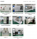
Dongguan Pasa Electronic Equipment Co., Ltd. is a professional semiconductor process equipment manufacturer integrating development, production and sales. It is a key backbone enterprise of China's high-end electronic industry basic equipment.
The company's main products are: special process equipment for semiconductor technology, special process equipment for electronic components, integrated circuit process equipment, special process equipment for solar cells, LED process equipment, gallium arsenide process equipment, nanomaterial process equipment, magnetic material process equipment, There are more than 100 types of special customized process equipment.
The company's main products are: special process equipment for semiconductor technology, special process equipment for electronic components, integrated circuit process equipment, special process equipment for solar cells, LED process equipment, gallium arsenide process equipment, nanomaterial process equipment, magnetic material process equipment, There are more than 100 types of special customized process equipment.

Companies that sell semiconductor-nanotech tools for R&D and possibly customized small batch production.
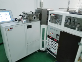
The also sell what looks like a really small sized Ion Implanter.
Low-energy ion implanter
The low-energy ion implanter can generate ultra-low-energy ion beams through the ion source. After being deflected by a dipole magnet, ions with different charge-to-mass ratios are filtered out, leaving only the required ion types and energies

Even more on thisThis thing is really interesting
first AI chip integrating memory & computing
sounds like this packages memory with computing unless I am missing something. @hvpc & @tokenanalyst have you seen advanced packaging of SRAM & processing units chiplets into chip. I would imagine this should already have happened with advanced packaging somwhere, right? bonding SRAM with CPU & GPU?
I see this
anyhow, aside from this, they also integrated it with CPU to have a full intelligent drive hardware platform
This really does seems like a very interesting approach. They first tried this computation in SRAM approach last year on a 22nm process. Now, they are able to generate even more powerful & efficient chip with 12nm process
so there is a well known issue where 60% of time is spent on data transfer and over 90% of power is used in data transfer. So my putting the computation unit inside SRAM (it's not clear how they are doing this), but they claim to greatly reduce # of calls into memory unit and computation unit, making it a lot more efficient. Didn't mission hybrid bonding or anything like this据悉,从现有芯片架构来看,超过60%时间是花在数据搬运上,超过90%的功耗也损失在数据搬运上。而存内计算技术利用存储器单元本身模拟或者物理性质完成计算,把原先存储器存储单元变成计算单元,可以大幅度减小计算单元调用次数,减少存储器次数,提高运算的效率。简而言之,存内计算运算单元就是存储单元本身,可以很好地解决存储墙、能耗墙得问题。
It's known that computation speed is advancing faster than memory bandwidth. By placing them close together, this just decreases the stale time of the computation unit. Alibaba Damo academy put memory/computation in 1 unit as a top 10 trend in 2023.与传统的冯诺依曼架构相比,存算一体打破了由于计算单元与存储单元过于独立而导致的“存储墙”和“功耗墙”,解决算力发展速度远超存储、存储带宽限制计算系统的速度等问题。今年1月,阿里巴巴达摩院甚至把存算一体列入了《2023十大科技趋势》。
Looks like this has been supported by 55 possible customers. From what I can see, this is not limited to autonomous driving. If they scale this up and make it on 7nm process, this could be a very powerful GPGPU
It seems like this is a very new concept, so there is a lot of improvement ahead still
before this instrument can be used as a production tool, we have to think about some practical things:Since ASML EUV with 13.5nm wave length can produce 7nm chips can this produce 3nm chips? , My knowledge is basic at best in this field btw
1. what about the absorption cross section of 6.7 nm vs 13.5 nm in typical photoresist?
2. what is the efficiency of the Gd vs Sn source?
3. what is the reflective efficiency of internal mirrors at 6.7 nm vs 13.5 nm?
yes, when it is done, it should halve the CD size, but even then CD is not purely dependent on wavelength. CD = k*L/NA where L is wavelength, NA is numerical aperture, k is a parameter of the system.
Status of various SMIC new fabs based on Q1 report. They will maintain capex.中芯国际发布2023年第一季度报告,公司依据扩产计划推进相应的资本开支。目前,中芯深圳已进入量产,中芯京城预计下半年进入量产,中芯东方预计年底通线,中芯西青还在建设中。面对市场的快速变化,公司将继续遵循以市场为导向、以客户为中心的策略,加强与终端市场的对话;全力配合新产品的推出,做好产线长短脚调整配套,迎接下一轮的增长周期。(格隆汇)
Shenzhen has started mass production
Jingcheng to enter mass product in 2nd half
Lingang to open line at end of this yr
Tianjin is still under construction
So it seems to me that Jingcheng has taken the longest to get up an running, because it's taken a lot of effort to test out de-americanized production lines. Hopefully, Lingang come online a lot faster.
Q1 capex was only 1.26B2023年第一季资本开支为12.586亿美元,研究及开发开支为1.677亿美元。一般及行政开支从2022年第四季的1.273亿美元减少至0.999亿美元。变动主要由于一控股新厂在2022年第四季投产,使本季度试经营相关开支减少。
capex maintaining earlier projection (last year's level), so expect Q2 capex to be high imo as it takes delivery of more ASML scanners before sanctions hit. Works out to be $5B for rest of the yr据介绍,公司依据扩产计划推进相应的资本开支。
the utilization dropped down to an unsightly 68%
monthly capacity increased to 732k 8-inch equivalent from 714k in Q4 and 649k a yr ago. Not the largest jump, but I think it's due a combination of already low utilization + delays in Jingcheng plant
They sold 1.251m wafers in Q1 vs 1.574m in Q4 and 1.84m a yr ago(converted to 8-inch wafer, so keep that in mind)
Revenue was $1.46B in Q1 vs 1.62B in Q4 and 1.84B a yr ago
That means revenue per 8-inch wafer has gone up from
$1000/wafer a year ago to $1029/wafer in Q4 to $1167/wafer in Q1
Since I doubt the price per wafer has really gone up. More likely went down. I think this is likely due to two factors:
1) Higher Finfet sales as % of overall sales -> its Finfet production likely fully booked and slowly increasing in capacity
2) Achieving higher wafer prices on more advanced process like 12/14nm through getting higher yield and more complexity on them
thoughts?
Last edited:
Any idea on the nodes in the facilities?
Status of various SMIC new fabs based on Q1 report. They will maintain capex.
Shenzhen has started mass production
Jingcheng to enter mass product in 2nd half
Lingang to open line at end of this yr
Tianjin is still under construction
So it seems to me that Jingcheng has taken the longest to get up an running, because it's taken a lot of effort to test out de-americanized production lines. Hopefully, Lingang come online a lot faster.
Link?
28nm. De-Americanized line.Any idea on the nodes in the facilities?
Status of various SMIC new fabs based on Q1 report. They will maintain capex.
Shenzhen has started mass production
Jingcheng to enter mass product in 2nd half
Lingang to open line at end of this yr
Tianjin is still under construction
So it seems to me that Jingcheng has taken the longest to get up an running, because it's taken a lot of effort to test out de-americanized production lines. Hopefully, Lingang come online a lot faster.
Q1 capex was only 1.26B
capex maintaining earlier projection (last year's level), so expect Q2 capex to be high imo as it takes delivery of more ASML scanners before sanctions hit. Works out to be $5B for rest of the yr
the utilization dropped down to an unsightly 68%
monthly capacity increased to 732k 8-inch equivalent from 714k in Q4 and 649k a yr ago. Not the largest jump, but I think it's due a combination of already low utilization + delays in Jingcheng plant
They sold 1.251m wafers in Q1 vs 1.574m in Q4 and 1.84m a yr ago(converted to 8-inch wafer, so keep that in mind)
Revenue was $1.46B in Q1 vs 1.62B in Q4 and 1.84B a yr ago
That means revenue per 8-inch wafer has gone up from
$1000/wafer a year ago to $1029/wafer in Q4 to $1167/wafer in Q1
Since I doubt the price per wafer has really gone up. More likely went down. I think this is likely due to two factors:
1) Higher Finfet sales as % of overall sales -> its Finfet production likely fully booked and slowly increasing in capacity
2) Achieving higher wafer prices on more advanced process like 12/14nm through getting higher yield and more complexity on them
thoughts?
Your theory on higher FinFET sales resulting in higher ASP makes sense. But that’s not it.
Status of various SMIC new fabs based on Q1 report. They will maintain capex.
Shenzhen has started mass production
Jingcheng to enter mass product in 2nd half
Lingang to open line at end of this yr
Tianjin is still under construction
So it seems to me that Jingcheng has taken the longest to get up an running, because it's taken a lot of effort to test out de-americanized production lines. Hopefully, Lingang come online a lot faster.
Q1 capex was only 1.26B
capex maintaining earlier projection (last year's level), so expect Q2 capex to be high imo as it takes delivery of more ASML scanners before sanctions hit. Works out to be $5B for rest of the yr
the utilization dropped down to an unsightly 68%
monthly capacity increased to 732k 8-inch equivalent from 714k in Q4 and 649k a yr ago. Not the largest jump, but I think it's due a combination of already low utilization + delays in Jingcheng plant
They sold 1.251m wafers in Q1 vs 1.574m in Q4 and 1.84m a yr ago(converted to 8-inch wafer, so keep that in mind)
Revenue was $1.46B in Q1 vs 1.62B in Q4 and 1.84B a yr ago
That means revenue per 8-inch wafer has gone up from
$1000/wafer a year ago to $1029/wafer in Q4 to $1167/wafer in Q1
Since I doubt the price per wafer has really gone up. More likely went down. I think this is likely due to two factors:
1) Higher Finfet sales as % of overall sales -> its Finfet production likely fully booked and slowly increasing in capacity
2) Achieving higher wafer prices on more advanced process like 12/14nm through getting higher yield and more complexity on them
thoughts?
There were several questions regarding the ASP during the investor call. The answer from SMIC CFO(?) was that it’s partially due to lower 8” order/utilization and higher price from rush orders for new products in 12”.
I recommend you listen to the call…(1hr). They also talked about their strategy on what product to focus on for their new fabs.
- Status
- Not open for further replies.
