Chinese semiconductor industry

Status
Not open for further replies.

FairAndUnbiased

Brigadier
Registered Member
Thank you, I understand.

I guess the issue here is just a lack of experience. As firms use domestic tools more and more, expertise will build, as well as the feedback loops necessary for maintaining reliability.
Not lack of experience as in, lack of skill due to experience.

It's that you literally will not find a 20k hour MTBF failure mode in a big piece of equipment without actually running the equipment for 20k hours. It's not like a chip that you can accelerated test in a chamber.
 

tphuang

Lieutenant General
Staff member
Super Moderator
VIP Professional
Registered Member
AMD had already announced v stacking of SRAM on top of CPU a few years ago, which you had already a link with some info on it. But this is not so prevalent because hybrid bonding/wafer bonding is quite expensive. it probably won’t see wide adoption until the 2nm or 1.4nm node.

as for the H30 chip, I can’t really tell what is going on there based solely on the article. Besides mentioning SRAM, I can’t tell for sure if hybrid bonding was used.
Great. I guess there could be a chance they are doing something special here that hasn't been successfully developed by other domestic players

In terms of AI development, having success bonding them together may allow you to have better performance. Which has applications beyond just autonomous driving. You could bind more complicated GPUs with SRAM for your GPGPU

I have hear MRAM and RRAM as alternatives in compute on memory applications no so much SRAM or DRAM but I think putting memory closer will help making computing faster.
In the case of SRAM, Samsung.

Please, Log in or Register to view URLs content!
Right I think it would be interesting to see what they can do here in terms of packaging to significantly improve performance. If you don't have 4nm process, but can stack SRAM
In China the company "IC league" has technology for heterogenous integration of DRAM and logic.

Please, Log in or Register to view URLs content!
yes, you provided this link earlier. There does seem to be some real advantage bounding DRAM and logic, but this is the first time I read about SRAM and logic. Hence my curiosity

According to feedback I received from the fabs, issue with domestic etchers and deposition is ‘reliability’.

everyone recognizes we have domestic tools (except scanner) that could do the job for 28nm logic, 128L 3D NAND, and 10G3 (D1x) DRAM. But tool reliability is not up to par with foreign tools of record….yet.

reliability=tool performing at the same level consistently over time; tool uptime

In our business, an equipment that is consistently bad is better than equipment that are inconsistently good. The first type, we can apply a correction via a feedback loop to address the “bad” part. The latter is simply a headache in an HVM setting. There’s nothing we can do with random inconsistencies on a production line.
I see, the thing is based on previous news, I think they already have or will soon have domestic non-scanner tools in 28nm logic & 128L 3D nand for HVM. I thought you said they did not even have anything to try HVM with 19nm DRAM. So if they do have something they can use now (even if at much worse reliability), this is something that can be improved over time.

Given how much favoritism CXMT has received, I don't think it's too much to ask for them to try domestic tools in their 21nm or 19nm process.
 
Last edited:

tonyget

Senior Member
Registered Member
Deposition equipment doesn't necessarily go by process node CD, only by process node chemical requirements.

Apparently it does go by process node CD

Please, Log in or Register to view URLs content!

 拓荆科技是目前国内唯一产业化应用集成电路PECVD 和SACVD 设备的厂商,也是国内领先的ALD 设备厂商。公司是国内半导体CVD 设备龙头,主要产品包括等离子体增强化学气相沉积(PECVD)设备、原子层沉积(ALD)设备和次常压化学气相沉积(SACVD)设备三个产品系列,是国内唯一产业化应用集成电路PECVD 和SACVD 设备的厂商,也是国内领先的ALD 设备厂商,已配适180-14nm 逻辑芯片、19/17nm DRAM 及64/128 层FLASH 制造工艺需求,广泛应用于中芯国际、华虹集团、长江存储、长鑫存储、厦门联芯、燕东微电子等国内主流晶圆厂产线,打破了国际厂商对国内市场的垄断。2021 年公司实现营业收入7.58 亿元,其中PECVD/SACVD/ALD 设备收入分别为6.75/0.41/0.29 亿元,营收占比分别为89.1%/5.4%/3.8%。

  公司PECVD 领先优势明显,ALD 和SACVD 将成为新的增长点。薄膜沉积设备作为晶圆制造的三大主设备之一,2020 年其投资规模占晶圆制造设备总投资的25%,仅次于刻蚀设备,其中PECVD、ALD 和SACVD 在薄膜沉积设备市场份额占比分别为33%、11%和小于6%,PECVD 设备占比最大。公司主要产品为PECVD、ALD 和SACVD,卡位优势明显。其中PECVD 设备在28nm 及以上制程逻辑产线基本可以实现各类薄膜工艺的覆盖,14nm 先进制程节点在验证中;PEALD 设备可以覆盖逻辑芯片55-14nm SADP、STI 工艺及存储领域,已实现产业化应用,ThermalALD 主要应用于28nm 以下制程逻辑芯片,正在研发中;SACVD 设备可以覆盖12 英寸40/28nm 以及8 英寸90nm 以上的逻辑芯片制造工艺需求。未来ALD 和SACVD 将逐步进入放量期,有望成为公司新的增长点。

Tuojing Technology is currently the only manufacturer of PECVD and SACVD equipment for industrialized application integrated circuits in China, and is also a leading ALD equipment manufacturer in China. The company is a leader in semiconductor CVD equipment in China. Its main products include plasma-enhanced chemical vapor deposition (PECVD) equipment, atomic layer deposition (ALD) equipment and sub-atmospheric chemical vapor deposition (SACVD) equipment. It is the only domestic industrialized A manufacturer of PECVD and SACVD equipment for applied integrated circuits, and a leading ALD equipment manufacturer in China. It has been adapted to the manufacturing process requirements of 180-14nm logic chips, 19/17nm DRAM and 64/128-layer FLASH, and is widely used in SMIC, Hua Hong The production lines of domestic mainstream fabs such as Group, Yangtze River Storage, Changxin Storage, Xiamen Lianxin, and Yandong Microelectronics have broken the monopoly of international manufacturers on the domestic market. In 2021, the company will achieve operating income of 758 million yuan, of which PECVD/SACVD/ALD equipment revenue will be 6.75/0.41/0.29 billion yuan, accounting for 89.1%/5.4%/3.8% of revenue.

The company has obvious leading advantages in PECVD, and ALD and SACVD will become new growth points. Thin film deposition equipment is one of the three main equipments for wafer manufacturing. Its investment scale accounts for 25% of the total investment in wafer manufacturing equipment in 2020, second only to etching equipment. Among them, PECVD, ALD and SACVD have the largest market share of thin film deposition equipment The proportions are 33%, 11% and less than 6% respectively, and PECVD equipment accounts for the largest proportion. The company's main products are PECVD, ALD and SACVD, with obvious card position advantages. Among them, PECVD equipment can basically realize the coverage of various thin film processes in the logic production line of 28nm and above processes, and the 14nm advanced process node is under verification; PEALD equipment can cover logic chip 55-14nm SADP, STI process and storage fields, and has achieved industrialization Application, ThermalALD is mainly used in logic chips with processes below 28nm and is under development; SACVD equipment can cover the manufacturing process requirements of 12-inch 40/28nm and 8-inch logic chips above 90nm. In the future, ALD and SACVD will gradually enter the heavy-duty period and are expected to become new growth points for the company.
 

latenlazy

Brigadier
Not lack of experience as in, lack of skill due to experience.

It's that you literally will not find a 20k hour MTBF failure mode in a big piece of equipment without actually running the equipment for 20k hours. It's not like a chip that you can accelerated test in a chamber.
Not even lack of skill per se. I would characterize it mostly as basic product maturity. You can have all the skills and experiences you need to quickly resolve edge cases but you simply don't know what you have to solve for if the problem hasn't emerged yet. That's just the nature of reliability engineering. It's an inherently time consuming process with a long maturation curve. This is why no one likes adopting new equipment unless it offers immense value in performance, and why even then new equipment product lines are often better deployed with smaller or more niche customers who wouldn't mind the occasional reliability penalties.
 

tokenanalyst

Brigadier
Registered Member
Shanghai Silicon Technology Taicang Ceramics Factory is about to be put into operation

The ceramic precision production line of Shanghai Silicon Precision Ceramics Technology (Suzhou) Co., Ltd. (hereinafter referred to as Shanghai Silicon Technology) will be officially put into operation on May 8, 2023 in the factory area of Shuangfeng Town, Taicang City.

Shanghai Silicon Technology Taicang Factory is a ceramic processing production line integrating high-temperature sintering furnace, precision grinding machine, CNC center, component cleaning line, and dust-free workshop. The factory also has an advanced ceramic research and development center to continuously innovate product types .

Shanghai Silicon Technology Taicang Ceramics Factory is about to be put into operation


Shanghai Silicon Technology is composed of a team with the background of the Institute of Ceramics of the Chinese Academy of Sciences, the Institute of Microsystems, and Shanghai Jiaotong University who have experience in R&D and manufacturing of the world's top 500 and American semiconductor equipment. Master the interdisciplinary core technical capabilities of special ceramic powder formula , preparation process , core equipment manufacturing , and precision machining . Committed to the research and production of precision ceramic parts for semiconductor equipment, including core equipment involving special working conditions (such as etching machines, CVD film deposition), as well as customized services for equipment companies . With the four advantages of its talent team, processing equipment, research and development application, and quality control, the company is constantly moving forward in the direction of becoming a top brand in the industry.

The Taicang plant of Shanghai Silicon Technology was put into operation, marking a key step for the company in the application of precision ceramics in the semiconductor industry. Through advanced production capacity equipment, personnel training, team building and quality control, the company will continue to explore and innovate, improve the quality and performance of precision ceramic products, and make greater contributions to the development of China's high-end application precision ceramic industry.

Please, Log in or Register to view URLs content!
 

latenlazy

Brigadier
Apparently it does go by process node CD

Please, Log in or Register to view URLs content!

 拓荆科技是目前国内唯一产业化应用集成电路PECVD 和SACVD 设备的厂商,也是国内领先的ALD 设备厂商。公司是国内半导体CVD 设备龙头,主要产品包括等离子体增强化学气相沉积(PECVD)设备、原子层沉积(ALD)设备和次常压化学气相沉积(SACVD)设备三个产品系列,是国内唯一产业化应用集成电路PECVD 和SACVD 设备的厂商,也是国内领先的ALD 设备厂商,已配适180-14nm 逻辑芯片、19/17nm DRAM 及64/128 层FLASH 制造工艺需求,广泛应用于中芯国际、华虹集团、长江存储、长鑫存储、厦门联芯、燕东微电子等国内主流晶圆厂产线,打破了国际厂商对国内市场的垄断。2021 年公司实现营业收入7.58 亿元,其中PECVD/SACVD/ALD 设备收入分别为6.75/0.41/0.29 亿元,营收占比分别为89.1%/5.4%/3.8%。

  公司PECVD 领先优势明显,ALD 和SACVD 将成为新的增长点。薄膜沉积设备作为晶圆制造的三大主设备之一,2020 年其投资规模占晶圆制造设备总投资的25%,仅次于刻蚀设备,其中PECVD、ALD 和SACVD 在薄膜沉积设备市场份额占比分别为33%、11%和小于6%,PECVD 设备占比最大。公司主要产品为PECVD、ALD 和SACVD,卡位优势明显。其中PECVD 设备在28nm 及以上制程逻辑产线基本可以实现各类薄膜工艺的覆盖,14nm 先进制程节点在验证中;PEALD 设备可以覆盖逻辑芯片55-14nm SADP、STI 工艺及存储领域,已实现产业化应用,ThermalALD 主要应用于28nm 以下制程逻辑芯片,正在研发中;SACVD 设备可以覆盖12 英寸40/28nm 以及8 英寸90nm 以上的逻辑芯片制造工艺需求。未来ALD 和SACVD 将逐步进入放量期,有望成为公司新的增长点。

Tuojing Technology is currently the only manufacturer of PECVD and SACVD equipment for industrialized application integrated circuits in China, and is also a leading ALD equipment manufacturer in China. The company is a leader in semiconductor CVD equipment in China. Its main products include plasma-enhanced chemical vapor deposition (PECVD) equipment, atomic layer deposition (ALD) equipment and sub-atmospheric chemical vapor deposition (SACVD) equipment. It is the only domestic industrialized A manufacturer of PECVD and SACVD equipment for applied integrated circuits, and a leading ALD equipment manufacturer in China. It has been adapted to the manufacturing process requirements of 180-14nm logic chips, 19/17nm DRAM and 64/128-layer FLASH, and is widely used in SMIC, Hua Hong The production lines of domestic mainstream fabs such as Group, Yangtze River Storage, Changxin Storage, Xiamen Lianxin, and Yandong Microelectronics have broken the monopoly of international manufacturers on the domestic market. In 2021, the company will achieve operating income of 758 million yuan, of which PECVD/SACVD/ALD equipment revenue will be 6.75/0.41/0.29 billion yuan, accounting for 89.1%/5.4%/3.8% of revenue.

The company has obvious leading advantages in PECVD, and ALD and SACVD will become new growth points. Thin film deposition equipment is one of the three main equipments for wafer manufacturing. Its investment scale accounts for 25% of the total investment in wafer manufacturing equipment in 2020, second only to etching equipment. Among them, PECVD, ALD and SACVD have the largest market share of thin film deposition equipment The proportions are 33%, 11% and less than 6% respectively, and PECVD equipment accounts for the largest proportion. The company's main products are PECVD, ALD and SACVD, with obvious card position advantages. Among them, PECVD equipment can basically realize the coverage of various thin film processes in the logic production line of 28nm and above processes, and the 14nm advanced process node is under verification; PEALD equipment can cover logic chip 55-14nm SADP, STI process and storage fields, and has achieved industrialization Application, ThermalALD is mainly used in logic chips with processes below 28nm and is under development; SACVD equipment can cover the manufacturing process requirements of 12-inch 40/28nm and 8-inch logic chips above 90nm. In the future, ALD and SACVD will gradually enter the heavy-duty period and are expected to become new growth points for the company.
Lol those are marketing labels to sell viability of application, not the technical performance parameters of the equipment. It's like saying a commercial plane engine can be used for this plane size or that plane size. The plane size is not the technical parameter by which the engine's performance is gauged. Only patterning related equipment defines technical performance around feature resolution, since that's the physical parameter patterning is geared towards.
 

FairAndUnbiased

Brigadier
Registered Member
Apparently it does go by process node CD

Please, Log in or Register to view URLs content!

 拓荆科技是目前国内唯一产业化应用集成电路PECVD 和SACVD 设备的厂商,也是国内领先的ALD 设备厂商。公司是国内半导体CVD 设备龙头,主要产品包括等离子体增强化学气相沉积(PECVD)设备、原子层沉积(ALD)设备和次常压化学气相沉积(SACVD)设备三个产品系列,是国内唯一产业化应用集成电路PECVD 和SACVD 设备的厂商,也是国内领先的ALD 设备厂商,已配适180-14nm 逻辑芯片、19/17nm DRAM 及64/128 层FLASH 制造工艺需求,广泛应用于中芯国际、华虹集团、长江存储、长鑫存储、厦门联芯、燕东微电子等国内主流晶圆厂产线,打破了国际厂商对国内市场的垄断。2021 年公司实现营业收入7.58 亿元,其中PECVD/SACVD/ALD 设备收入分别为6.75/0.41/0.29 亿元,营收占比分别为89.1%/5.4%/3.8%。

  公司PECVD 领先优势明显,ALD 和SACVD 将成为新的增长点。薄膜沉积设备作为晶圆制造的三大主设备之一,2020 年其投资规模占晶圆制造设备总投资的25%,仅次于刻蚀设备,其中PECVD、ALD 和SACVD 在薄膜沉积设备市场份额占比分别为33%、11%和小于6%,PECVD 设备占比最大。公司主要产品为PECVD、ALD 和SACVD,卡位优势明显。其中PECVD 设备在28nm 及以上制程逻辑产线基本可以实现各类薄膜工艺的覆盖,14nm 先进制程节点在验证中;PEALD 设备可以覆盖逻辑芯片55-14nm SADP、STI 工艺及存储领域,已实现产业化应用,ThermalALD 主要应用于28nm 以下制程逻辑芯片,正在研发中;SACVD 设备可以覆盖12 英寸40/28nm 以及8 英寸90nm 以上的逻辑芯片制造工艺需求。未来ALD 和SACVD 将逐步进入放量期,有望成为公司新的增长点。

Tuojing Technology is currently the only manufacturer of PECVD and SACVD equipment for industrialized application integrated circuits in China, and is also a leading ALD equipment manufacturer in China. The company is a leader in semiconductor CVD equipment in China. Its main products include plasma-enhanced chemical vapor deposition (PECVD) equipment, atomic layer deposition (ALD) equipment and sub-atmospheric chemical vapor deposition (SACVD) equipment. It is the only domestic industrialized A manufacturer of PECVD and SACVD equipment for applied integrated circuits, and a leading ALD equipment manufacturer in China. It has been adapted to the manufacturing process requirements of 180-14nm logic chips, 19/17nm DRAM and 64/128-layer FLASH, and is widely used in SMIC, Hua Hong The production lines of domestic mainstream fabs such as Group, Yangtze River Storage, Changxin Storage, Xiamen Lianxin, and Yandong Microelectronics have broken the monopoly of international manufacturers on the domestic market. In 2021, the company will achieve operating income of 758 million yuan, of which PECVD/SACVD/ALD equipment revenue will be 6.75/0.41/0.29 billion yuan, accounting for 89.1%/5.4%/3.8% of revenue.

The company has obvious leading advantages in PECVD, and ALD and SACVD will become new growth points. Thin film deposition equipment is one of the three main equipments for wafer manufacturing. Its investment scale accounts for 25% of the total investment in wafer manufacturing equipment in 2020, second only to etching equipment. Among them, PECVD, ALD and SACVD have the largest market share of thin film deposition equipment The proportions are 33%, 11% and less than 6% respectively, and PECVD equipment accounts for the largest proportion. The company's main products are PECVD, ALD and SACVD, with obvious card position advantages. Among them, PECVD equipment can basically realize the coverage of various thin film processes in the logic production line of 28nm and above processes, and the 14nm advanced process node is under verification; PEALD equipment can cover logic chip 55-14nm SADP, STI process and storage fields, and has achieved industrialization Application, ThermalALD is mainly used in logic chips with processes below 28nm and is under development; SACVD equipment can cover the manufacturing process requirements of 12-inch 40/28nm and 8-inch logic chips above 90nm. In the future, ALD and SACVD will gradually enter the heavy-duty period and are expected to become new growth points for the company.
1. You cited a finance source, not a scientific or engineering source. So we only know what financiers who are not subject matter experts call it based on your report. We don't know what actual scientists call it.

2. The critical dimension of a deposition process is the vertical dimension, not horizontal dimension, so it is meaningless to assign a horizontal dimension process node number to it.

3. I debunked you on exactly this topic on this exact thread last year when I showed 1990s Applied Materials tools can be used for GAAFET research.


4. Applied Material and Lam Research never go by process node in their CVD tools. They mention only deposition rate, deposition maximum thickness, wafer size, wafer throughput and deposition chemistry.

this every single Applied Materials CVD product and not a single one mentions process node.

Please, Log in or Register to view URLs content!

Please, Log in or Register to view URLs content!

Please, Log in or Register to view URLs content!

Please, Log in or Register to view URLs content!

Please, Log in or Register to view URLs content!

5. I personally have qualified etch and deposition chamber components based on industry standard methods like SEMI F60 and SEMI F72 as well as proprietary standards from leading OEMs like Applied Materials and Lam Research. These standard methods do not mention "xx nm process" anywhere.

Please, Log in or Register to view URLs content!
 

HighGround

Senior Member
Registered Member
5. I personally have qualified etch and deposition chamber components based on industry standard methods like SEMI F60 and SEMI F72 as well as proprietary standards from leading OEMs like Applied Materials and Lam Research. These standard methods do not mention "xx nm process" anywhere.

Please, Log in or Register to view URLs content!

Careful here. You never know, I might be making recommendations to the CIA. ;)

Thanks for the information as always, helpful in furthering my understanding of this industry.
 

tokenanalyst

Brigadier
Registered Member
Apparently it does go by process node CD

Please, Log in or Register to view URLs content!

 拓荆科技是目前国内唯一产业化应用集成电路PECVD 和SACVD 设备的厂商,也是国内领先的ALD 设备厂商。公司是国内半导体CVD 设备龙头,主要产品包括等离子体增强化学气相沉积(PECVD)设备、原子层沉积(ALD)设备和次常压化学气相沉积(SACVD)设备三个产品系列,是国内唯一产业化应用集成电路PECVD 和SACVD 设备的厂商,也是国内领先的ALD 设备厂商,已配适180-14nm 逻辑芯片、19/17nm DRAM 及64/128 层FLASH 制造工艺需求,广泛应用于中芯国际、华虹集团、长江存储、长鑫存储、厦门联芯、燕东微电子等国内主流晶圆厂产线,打破了国际厂商对国内市场的垄断。2021 年公司实现营业收入7.58 亿元,其中PECVD/SACVD/ALD 设备收入分别为6.75/0.41/0.29 亿元,营收占比分别为89.1%/5.4%/3.8%。

  公司PECVD 领先优势明显,ALD 和SACVD 将成为新的增长点。薄膜沉积设备作为晶圆制造的三大主设备之一,2020 年其投资规模占晶圆制造设备总投资的25%,仅次于刻蚀设备,其中PECVD、ALD 和SACVD 在薄膜沉积设备市场份额占比分别为33%、11%和小于6%,PECVD 设备占比最大。公司主要产品为PECVD、ALD 和SACVD,卡位优势明显。其中PECVD 设备在28nm 及以上制程逻辑产线基本可以实现各类薄膜工艺的覆盖,14nm 先进制程节点在验证中;PEALD 设备可以覆盖逻辑芯片55-14nm SADP、STI 工艺及存储领域,已实现产业化应用,ThermalALD 主要应用于28nm 以下制程逻辑芯片,正在研发中;SACVD 设备可以覆盖12 英寸40/28nm 以及8 英寸90nm 以上的逻辑芯片制造工艺需求。未来ALD 和SACVD 将逐步进入放量期,有望成为公司新的增长点。

Tuojing Technology is currently the only manufacturer of PECVD and SACVD equipment for industrialized application integrated circuits in China, and is also a leading ALD equipment manufacturer in China. The company is a leader in semiconductor CVD equipment in China. Its main products include plasma-enhanced chemical vapor deposition (PECVD) equipment, atomic layer deposition (ALD) equipment and sub-atmospheric chemical vapor deposition (SACVD) equipment. It is the only domestic industrialized A manufacturer of PECVD and SACVD equipment for applied integrated circuits, and a leading ALD equipment manufacturer in China. It has been adapted to the manufacturing process requirements of 180-14nm logic chips, 19/17nm DRAM and 64/128-layer FLASH, and is widely used in SMIC, Hua Hong The production lines of domestic mainstream fabs such as Group, Yangtze River Storage, Changxin Storage, Xiamen Lianxin, and Yandong Microelectronics have broken the monopoly of international manufacturers on the domestic market. In 2021, the company will achieve operating income of 758 million yuan, of which PECVD/SACVD/ALD equipment revenue will be 6.75/0.41/0.29 billion yuan, accounting for 89.1%/5.4%/3.8% of revenue.

The company has obvious leading advantages in PECVD, and ALD and SACVD will become new growth points. Thin film deposition equipment is one of the three main equipments for wafer manufacturing. Its investment scale accounts for 25% of the total investment in wafer manufacturing equipment in 2020, second only to etching equipment. Among them, PECVD, ALD and SACVD have the largest market share of thin film deposition equipment The proportions are 33%, 11% and less than 6% respectively, and PECVD equipment accounts for the largest proportion. The company's main products are PECVD, ALD and SACVD, with obvious card position advantages. Among them, PECVD equipment can basically realize the coverage of various thin film processes in the logic production line of 28nm and above processes, and the 14nm advanced process node is under verification; PEALD equipment can cover logic chip 55-14nm SADP, STI process and storage fields, and has achieved industrialization Application, ThermalALD is mainly used in logic chips with processes below 28nm and is under development; SACVD equipment can cover the manufacturing process requirements of 12-inch 40/28nm and 8-inch logic chips above 90nm. In the future, ALD and SACVD will gradually enter the heavy-duty period and are expected to become new growth points for the company.
It goes more for the range of material that is capable of deposit and the ways can deposit certain materials for certain manufacturing process. BUT is true that deposition equipment is also rated to work with certain RANGE of node process or devices, MEMS, packaging, photonics and so on depending on certain factors.

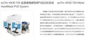
for example this specifically says is for Titanium and Titanium Nitride, the process range is 55-28nm and for Hardmask, it could be used to 14nm but was not designed with that process in mind.

1683752162305.png

this is more for epitaxial deposition of crystals materials with low defectivity used in NAND and Logic circuits.

Please, Log in or Register to view URLs content!

The node process naming is defined by the lithography process not even the lithography machine itself. But lately has become a commercial gimick.
 
Last edited:

FairAndUnbiased

Brigadier
Registered Member
Careful here. You never know, I might be making recommendations to the CIA. ;)

Thanks for the information as always, helpful in furthering my understanding of this industry.
There are probably 10k+ people in the US alone who know how to qualify tools and components following SEMI and internal standards. it's not super or rare.

Coming up with those standards? Much harder. Just like pilots are pretty smart but the guys who built the plane are geniuses.
 
Status
Not open for further replies.
Top