Chinese semiconductor industry

Status
Not open for further replies.

PopularScience

Junior Member
Registered Member
You must be confused by CXMT’s marketing.

CXMT referred to their first generation DRAM as “1x”. But over time they had admitted it is equivalent to what the industry called “D20” that’s roughly 23nm node.

Their second HVM node, which CXMT and media calls “D1y” is actually what industry calls D1x (based on its bitline, wordline pitch). Based on the actual design pitch, this would be closer to 19nm node.

They currently developing their third generation DRAM node, 16-17nm, is still in development. As of today 2023 they are still trying to developing this. It’s not in production.

the media was duped by CXMT’s node naming before CXMT admitted to the industry on what they are really producing. If you are referring to some media report from 2021 then you are a bit outdated.

min the industry, we benchmark what fabs call their nodes by looking at and compare the actual design dimensions. My assessment and the article claiming 4 generation behind are based on this method.

but, buddy, you are free to believe in your own version of truth. I’m simply providing the standard assessment of the industry. Everyone else has the freedom decide which contradicting info to believe in. Just doing my part to share an “alternate” view.

D1x lack behind Samsung D1x doesn't mean D1y lack behind Samsung D1y
 

tphuang

Lieutenant General
Staff member
Super Moderator
VIP Professional
Registered Member
Please, Log in or Register to view URLs content!
Houmo.AI has unveiled H30 HaloDrive SoC for EVs. It does 256TOPS, consumes just 35W of power and uses 12nm process.
This is actually not bad.

put things into perspective, journey 5 uses 16nm process and does 128 TOPS
This thing is really interesting
Please, Log in or Register to view URLs content!
后摩智能正式发布首款存算一体智驾芯片——鸿途™H30,最高物理算力 256TOPS,典型功耗 35W,成为国内率先落地存算一体大算力 AI 芯片的公司。
first AI chip integrating memory & computing
鸿途™H30 以存算一体创新架构实现了六大技术突破,即大算力、全精度、低功耗、车规级、可量产、通用性。鸿途™H30 基于 SRAM 存储介质,采用数字存算一体架构,拥有极低的访存功耗和超高的计算密度,在 Int8 数据精度条件下,其 AI 核心IPU 能效比高达 15Tops/W,是传统架构芯片的7 倍以上
sounds like this packages memory with computing unless I am missing something. @hvpc & @tokenanalyst have you seen advanced packaging of SRAM & processing units chiplets into chip. I would imagine this should already have happened with advanced packaging somwhere, right? bonding SRAM with CPU & GPU?
I see this
Please, Log in or Register to view URLs content!


anyhow, aside from this, they also integrated it with CPU to have a full intelligent drive hardware platform
本次发布会,后摩智能同步推出了基于鸿途™H30 芯片打造的智能驾驶硬件平台——力驭®。有赖于鸿途™H30极高的计算效率和计算密度,力驭®平台 CPU 算力高达200 Kdmips,AI 算力高 256Tops,支持多传感器输入,能够为智能驾驶提供更充沛的算力支持,进一步提升了系统的可靠性。力驭®平台功耗仅为 85W,可采用更加灵活的散热方式,实现更低成本的便捷部署,有利于推动大算力智能驾驶场景的普及应用。
 

hvpc

Junior Member
Registered Member
Which part of afticle mentioned this is 19nm aka 1x?
@PopularScience, I’m not interested in a debate to convince you of the truth nor am I interested in spoon feeding you and walk you through step by step.

I’ll just say this, You certainly are aware CXMT started out with their 10G1 “19nm” node. They didn’t make anything older than 10G1.
If you can’t deduce that TechInsight assessment is on 10G1, which they correctly assessed as 22nm then please go ahead and keep believing in whatever you read in the news.

I’m certainly not about to share the GDS file containing every layer of 10G1 design layout with the exact CD feature size just to prove my point; I’m not about reveal any more details beyond what I already shared.
 

ZeEa5KPul

Colonel
Registered Member
@PopularScience, I’m not interested in a debate to convince you of the truth
Then don't post anything. It's poor form to go "trust me, bro" when your assertions are called out.
I’m certainly not about to share the GDS file containing every layer of 10G1 design layout with the exact CD feature size just to prove my point
What point? If you don't back your assertions with evidence, you haven't made any point.
 

european_guy

Junior Member
Registered Member

Zhongwei Company launched a 12-inch thin film deposition equipment!​


Recently, AMEC Semiconductor Equipment (Shanghai) Co., Ltd. (hereinafter referred to as "AMEC", Shanghai Stock Exchange Stock Code: 688012) launched the self-developed 12-inch low-pressure chemical vapor deposition (LPCVD) equipment Preforma Uniflex™ CW. This is a new breakthrough made by China Microelectronics in the field of semiconductor thin film deposition, which has been deeply involved in high-end micro-processing equipment for many years, and it is also a new momentum to realize the diversified growth of the company's business.

As a 12-inch LPCVD equipment with high output efficiency and excellent performance independently developed by AMEC, Preforma Uniflex™ CW can flexibly configure up to five double reaction chambers (ten reaction chambers), and each reaction chamber can process simultaneously Two wafers, while ensuring lower production costs and chemical consumption, achieve higher production efficiency.

Preforma Uniflex™ CW, as an LPCVD equipment independently developed by AMEC, is equipped with an optimized gas mixing solution and heating stage with completely independent intellectual property rights. It has excellent film uniformity, filling ability and process adjustment flexibility. Large wafers, it also has good process capabilities. And its excellent step coverage and filling ability can meet the application requirements of filling contact holes and metal tungsten lines in advanced logic devices, DRAM and 3D NAND.

The Preforma Uniflex™ CW launched by AMEC is another milestone in the company's road to innovation. "This LPCVD equipment not only has complete and independent intellectual property rights, but also created a new record for the speed of research and development of new equipment in China Microelectronics." Said Tao Heng, Vice President of China Microelectronics Group, General Manager of LPCVD Product Department and Public Platform Engineering Department: "Since the establishment of this LPCVD equipment research and development project, we have completed product design, production prototype development and laboratory evaluation in less than half a year, and have successfully imported it to the client for production line approval."

View attachment 112365
Please, Log in or Register to view URLs content!


After Naura and Piotech, now also AMEC builds CVD equipment. CVD field is getting crowded :)

Unfortunately there is no mention to supported process node, just that "can meet the application requirements of filling contact holes and metal tungsten lines in advanced logic devices, DRAM and 3D NAND".
 

tokenanalyst

Brigadier
Registered Member
This thing is really interesting
Please, Log in or Register to view URLs content!

first AI chip integrating memory & computing

sounds like this packages memory with computing unless I am missing something. @hvpc & @tokenanalyst have you seen advanced packaging of SRAM & processing units chiplets into chip. I would imagine this should already have happened with advanced packaging somwhere, right? bonding SRAM with CPU & GPU?
I see this
Please, Log in or Register to view URLs content!


anyhow, aside from this, they also integrated it with CPU to have a full intelligent drive hardware platform
I have hear MRAM and RRAM as alternatives in compute on memory applications no so much SRAM or DRAM but I think putting memory closer will help making computing faster.
In the case of SRAM, Samsung.

Please, Log in or Register to view URLs content!

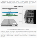
In China the company "IC league" has technology for heterogenous integration of DRAM and logic.
1683732700720.png

Please, Log in or Register to view URLs content!
 

tokenanalyst

Brigadier
Registered Member
After Naura and Piotech, now also AMEC sells CVD equipment. CVD field is getting crowded :)

Unfortunately there is no mention to supported process node, just that "can meet the application requirements of filling contact holes and metal tungsten lines in advanced logic devices, DRAM and 3D NAND".
Looks the are planning to sell this tools for memory applications and tungsten deposition, they looking to fill the gap with AMAT in the WCVD market, the W stand for tungsten which I don't think was available domestically in China before.

Please, Log in or Register to view URLs content!

AMEC main deposition product is MOCVD
Naura is good a PVD tools, sputtering and such.
Piotech which AMEC is an investor, is the only company in China selling sub-atmospheric chemical deposition tools, necessary for 3DNAND production.
LeadMicro is more in the ALD market of some dielectrics and photovoltaic.

Of course they have products that overlap which is good for competition but looks like everyone is trying to carve a niche market for their own.

I think for now AMEC with their MOCVD tools and now WCVD has made a niche market for their own in China.
 

tokenanalyst

Brigadier
Registered Member
And by the way tungsten deposition (W-CVD) is one of the technologies that the stooges think tankers were talking about in their big brain presentation in Washington D.C. to the Chicken-Hawk politicians before the ban on YMTC where they discussed equipment-materials for the production of semiconductor devices and obviously in a demonstration of knowledge of the industry they mostly talked about deposition equipment as if it were the only equipment used in a semiconductor factory, well, they ended up telling the politicians in D.C. that it was necessary to introduce export controls because China did not have this type of equipment, it seems that it did not age well.
 

hvpc

Junior Member
Registered Member
This thing is really interesting
Please, Log in or Register to view URLs content!

first AI chip integrating memory & computing

sounds like this packages memory with computing unless I am missing something. @hvpc & @tokenanalyst have you seen advanced packaging of SRAM & processing units chiplets into chip. I would imagine this should already have happened with advanced packaging somwhere, right? bonding SRAM with CPU & GPU?
I see this
Please, Log in or Register to view URLs content!


anyhow, aside from this, they also integrated it with CPU to have a full intelligent drive hardware platform
AMD had already announced v stacking of SRAM on top of CPU a few years ago, which you had already a link with some info on it. But this is not so prevalent because hybrid bonding/wafer bonding is quite expensive. it probably won’t see wide adoption until the 2nm or 1.4nm node.

as for the H30 chip, I can’t really tell what is going on there based solely on the article. Besides mentioning SRAM, I can’t tell for sure if hybrid bonding was used.
 
Status
Not open for further replies.
Top