Chinese semiconductor industry

Status
Not open for further replies.

tokenanalyst

Brigadier
Registered Member

Another semiconductor core equipment successfully broke through, and the domestic high-end thermostat solved the bottleneck problem​


Jiwei.com learned that not long ago, a leading supplier of photovoltaic equipment in China solved a key bottleneck - the cascade temperature controller dedicated to semiconductor equipment . The product successfully passed the production line verification of domestic photovoltaic leading It is a domestic alternative, and it is superior to foreign brand products in improving the photovoltaic yield rate. It has been rated as internationally advanced by industry experts in the national scientific and technological achievements appraisal.

1184082987789.363.jpg


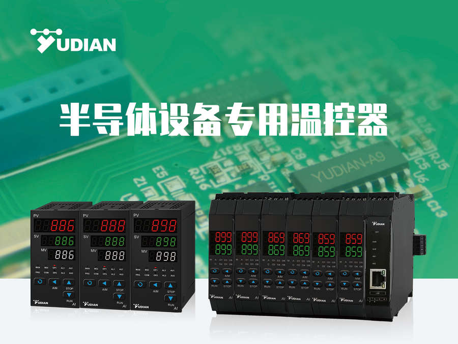
It is reported that the cascade thermostat is independently developed by Xiamen Yudian Automation Technology Co., Ltd. (hereinafter referred to as: Yudian), a domestic manufacturer that has been in the field of temperature control for more than 30 years . The successful launch of the domestic cascade thermostat for semiconductor equipment has filled the domestic gap in this field for many years. With the successful introduction in the photovoltaic manufacturing production line, this product will expand to a wider range of semiconductor manufacturing fields such as microelectronics, and promote the domestic substitution of upstream semiconductor equipment.

Replacing foreign brands, domestic thermostats achieve breakthroughs in the field of photovoltaic semiconductors

A thermostat, as the name suggests, is a device that measures and regulates temperature. It reads the measured value of the temperature sensor and executes a complex and intelligent control algorithm through a computer program, and uses connected actuators to precisely adjust the temperature of loads such as heaters. It is an essential core accessory for industrial production and automated production lines.

Unlike ordinary PID thermostats, cascade thermostats used in many links in semiconductor production equipment, such as diffusion, oxidation, etching, PECVD, etc., require high-end complex adjustment algorithms to deal with temperature control lag in semiconductor equipment Larger and more disturbance problems. As a high-end market for thermostat applications, the semiconductor manufacturing field has very strict requirements on the product accuracy, reliability, anti-interference and stability of thermostats.

An insider in the photovoltaic manufacturing industry pointed out that on the production line of crystalline silicon solar cells, temperature control is like the soul . For example, the diffusion furnace needs to heat the temperature in the furnace to about 700°C-1040°C according to a certain heating rate, and quickly stabilize the temperature fluctuation within ±0.5°C, which is extremely important for the accuracy, reliability and stability of temperature control. Strict requirements, once the temperature deviates, the product performance will be greatly reduced or even scrapped.

The ultra-high technical threshold makes it possible for only a handful of cascade thermostat manufacturers to enter the semiconductor field. In the past, only a few brands such as Japan's AZBIL, Britain's PMA, and America's WATLOW's EUROTHERM could meet the requirements. Yudian's newly launched AI-8 cascade thermostat for semiconductor equipment successfully entered the field of photovoltaic manufacturing last year, becoming the only domestic thermostat company whose products have passed the verification of the photovoltaic semiconductor market.

Please, Log in or Register to view URLs content!
 

hvpc

Junior Member
Registered Member
CXMT is D1y, 17nm.

长鑫19nm DDR4内存芯片良率已达75% ,17nm工艺爬升中​


Please, Log in or Register to view URLs content!
See my previous post. The CXMT “19nm” node here is not what the industry called 19nm. This is equivalent to 20ish nm node.

likewise, what CXMT called “17nm” is equivalent to what everyone called 19nm.

for a benchmark to make sense, you’d need to use the same metrics for comparison, not merely use the marketing naming convention.
 
Last edited:

tokenanalyst

Brigadier
Registered Member

Guangli Microelectronics EDA industrialization base project started smoothly​


On the morning of May 9th, the opening ceremony of Guangli Microelectronics EDA Industrialization Base Project was held in Binjiang District, Hangzhou. Government leaders of Binjiang District, experts and scholars in the integrated circuit industry, company shareholder representatives, staff representatives of Guangli Microelectronics and project construction units were in charge People at the event site witnessed the start of the project.

At the ceremony, Wang Lisheng, deputy director of the Management Committee of Hangzhou High-tech Zone, spoke highly of Guangliwei's outstanding contribution to the development of my country's integrated circuit industry as an industry-leading manufacturer of EDA software and wafer-level electrical testing equipment. Liwei can take the construction of the project as an opportunity to continue to cultivate and develop bravely, so as to empower the innovation and development of the integrated circuit industry in Hangzhou and even the whole country.

The project is positioned as the headquarters of Hangzhou Guangli Microelectronics Co., Ltd. and its R&D and production base. After the completion of the project, it can meet the office and research and development needs of more than 1,000 employees, and has the production capacity of more than 1,000 sets of WAT testing equipment per year. At that time, this industrialization base will inject strong momentum into the development of Guangliwei.

1683719746233.png

Please, Log in or Register to view URLs content!
 

hvpc

Junior Member
Registered Member
See my previous post. The CXMT “19nm” node here is not what the industry called 19nm. This is equivalent to 20ish nm node.

likewise, what CXMT called “17nm” is equivalent to what everyone called 19nm.

for a benchmark to make sense, you’d need to use the same metrics for comparison, not merely use the marketing naming convention.
@PopularScience, if you need more proof CXMT’s “19nm” is sandbagged, this is the assessment from TechInsight that echoes what I said.

TechInsight refers to CXMT’s first generation “19nm” DRAM as Samsung 22nm equivalent.

Please, Log in or Register to view URLs content!


The DRAM of today takes in a 6F2 design. Each bit cell takes up 6 “pixels” with dimension of ‘F’nm. The magnitude of ‘F’ dictates which DRAM node the design is. Despite CXMT originally, intentionally or not, trying to mislead the media, once people get a hold of their chip the truth will come out.

TechInsight clearly point out what I said, that CXMT’s first gen “19nm” is equivalent to Samsung 22nm.

If you have different information on the actual CXMT bitline pitch, wordline pitch, and Active pitch (used to determine actual design node) to dispute TechInsight and what I’m saying then I’ll be all ears, mate. But don’t go blindly believe what the media reports because they are, more often than not, wrong on the technical details.
 

tokenanalyst

Brigadier
Registered Member

Zhongwei Company launched a 12-inch thin film deposition equipment!​


Recently, AMEC Semiconductor Equipment (Shanghai) Co., Ltd. (hereinafter referred to as "AMEC", Shanghai Stock Exchange Stock Code: 688012) launched the self-developed 12-inch low-pressure chemical vapor deposition (LPCVD) equipment Preforma Uniflex™ CW. This is a new breakthrough made by China Microelectronics in the field of semiconductor thin film deposition, which has been deeply involved in high-end micro-processing equipment for many years, and it is also a new momentum to realize the diversified growth of the company's business.

As a 12-inch LPCVD equipment with high output efficiency and excellent performance independently developed by AMEC, Preforma Uniflex™ CW can flexibly configure up to five double reaction chambers (ten reaction chambers), and each reaction chamber can process simultaneously Two wafers, while ensuring lower production costs and chemical consumption, achieve higher production efficiency.

Preforma Uniflex™ CW, as an LPCVD equipment independently developed by AMEC, is equipped with an optimized gas mixing solution and heating stage with completely independent intellectual property rights. It has excellent film uniformity, filling ability and process adjustment flexibility. Large wafers, it also has good process capabilities. And its excellent step coverage and filling ability can meet the application requirements of filling contact holes and metal tungsten lines in advanced logic devices, DRAM and 3D NAND.

The Preforma Uniflex™ CW launched by AMEC is another milestone in the company's road to innovation. "This LPCVD equipment not only has complete and independent intellectual property rights, but also created a new record for the speed of research and development of new equipment in China Microelectronics." Said Tao Heng, Vice President of China Microelectronics Group, General Manager of LPCVD Product Department and Public Platform Engineering Department: "Since the establishment of this LPCVD equipment research and development project, we have completed product design, production prototype development and laboratory evaluation in less than half a year, and have successfully imported it to the client for production line approval."

1683727855841.png
Please, Log in or Register to view URLs content!


Alb

New Member
Registered Member
This is the roadmap that Samsung shared during their Memory Tech Day.

Someone had questions about whether China/CXMT could makd DDR5/GDDR5 awhile back. This chart should clearly give you an overview of where CXMT stands relative to others in the industry and what sort of product offering they could provide.

At the moment, CXMT is limited to the basic DDR4 & its low power varient, the LPDDR4x. The lagging technical capability is why CXMT is not able to and not advertising product offering in HBM, GDDR, CXL, or higher capacity and capability DDR/LPDDR chips.

And with the US BIS sanction on anything below D18 (D1x), this is also the reason why there's a lot of activities domestically to pursue 3D-DRAM architecture with the larger resolution. The industry as whole, instead are continuing the 2D shrink route and won't be forced to look into 3D-DRAM until D0b.

View attachment 112349

We may be at risk of falling behind more than 4 generations in DRAM as we optimize and qualify domestic equipment. At the current timeline, we may already be 5 generations behind in DRAM by the time domestic fabs figure out how to work with domestic. equipment.

With all the overhead we have to tackle, domestic DRAM fabs are simply not innovating at the same pace as the industry. It was the case before last Oct's US BIS sanction, it's even more difficult after the sanction.
JHICC have managed to de-americanize their DRAM 25nm production line. Do you know which extra tools are needed at 17nm compared to 25nm for DRAM. I am just trying to assess how hard it is to overcome the US restrictions for CXMT.
 

PopularScience

Junior Member
Registered Member
@PopularScience, if you need more proof CXMT’s “19nm” is sandbagged, this is the assessment from TechInsight that echoes what I said.

TechInsight refers to CXMT’s first generation “19nm” DRAM as Samsung 22nm equivalent.

Please, Log in or Register to view URLs content!


The DRAM of today takes in a 6F2 design. Each bit cell takes up 6 “pixels” with dimension of ‘F’nm. The magnitude of ‘F’ dictates which DRAM node the design is. Despite CXMT originally, intentionally or not, trying to mislead the media, once people get a hold of their chip the truth will come out.

TechInsight clearly point out what I said, that CXMT’s first gen “19nm” is equivalent to Samsung 22nm.

If you have different information on the actual CXMT bitline pitch, wordline pitch, and Active pitch (used to determine actual design node) to dispute TechInsight and what I’m saying then I’ll be all ears, mate. But don’t go blindly believe what the media reports because they are, more often than not, wrong on the technical details.

Which part of afticle mentioned this is 19nm aka 1x?
 

ansy1968

Brigadier
Registered Member
JHICC have managed to de-americanize their DRAM 25nm production line. Do you know which extra tools are needed at 17nm compared to 25nm for DRAM. I am just trying to assess how hard it is to overcome the US restrictions for CXMT.
Hello @Alb long time no hear, I hope you post more and give us more updates. :)
 
  • Like
Reactions: Alb
Status
Not open for further replies.
Top