Chinese semiconductor industry

Status
Not open for further replies.

tokenanalyst

Brigadier
Registered Member

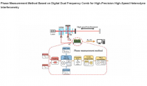
Phase Measurement Method Based on Digital Dual Frequency Comb for High-Precision High-Speed Heterodyne Interferometry​

School of Instrumentation Science and Engineering, Harbin Institute of Technology, Harbin, China
Key Laboratory of Ultraprecision Intelligent Instrumentation, Ministry of Industry and Information Technology, Harbin, China

Abstract:
The heterodyne interferometer is widely used as a precise displacement sensor in ultraprecision processing. However, there is a tradeoff between measurement speed and measurement precision in the existing interference signal processing methods. In this work, a novel phase measurement method based on digital dual frequency comb is proposed. The proposed method uses the intrinsic frequency comb signal and a narrowband low-pass filter to form a bandpass filter bank, which divides the broadband brought by high-speed movement into multiple narrow bands. The signal-to-noise ratio (SNR) is improved for phase calculation. In addition, two groups of intrinsic frequency comb signals are used simultaneously for phase measurement and the rotation of the output, preventing the inaccurate phase measurement of the input signal, whose frequency is the average of two frequencies in the frequency comb signal. The heterodyne laser interferometer can maintain high precision at high measurement speed. The simulation results show that the precision of the proposed method is more than 50% higher than that of the phase-locked loop method. The experiment with a circuit board combined with 100-Msps sampling 16-bit analog-to-digital converter (ADC) shows that the phase measurement precision of the input signal frequency in the bandwidth range of 2.5–37.5 MHz can reach 0.77 mrad, equivalent to the displacement measurement precision of the double-pass interferometer (19 pm) at a measurement speed of less than 2.77 m/s.
1683642369650.png
Please, Log in or Register to view URLs content!
 

tokenanalyst

Brigadier
Registered Member

Integrated optical critical dimension metrology with Mueller matrix ellipsometry​


aState Key Laboratory of Digital Manufacturing Equipment and Technology, Huazhong University of Science and Technology, Wuhan, ChinabWuhan Eoptics Technology Co. Ltd., Wuhan 430075, ChinacOptics Valley Laboratory, Wuhan 430074, China,

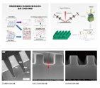
Mueller matrix ellipsometry (MME) is commonly applied by the standalone instruments in semiconductor manufacturing process for films and nanostructures characterization. However, MME is rarely used in the integrated metrology optical critical dimension (IM OCD) tools due to the difficulty in extracting the parameters under varied azimuth angle conditions, which is induced by the rotation of R-θ wafer stage adapted to the restricted space. When the measurements on a same wafer are achieved under multiple azimuthal angles, the measured nanostructure parameters usually mismatch the baseline values provided by the manufacturer, and therefore lead to the unacceptable accuracy loss. In this paper, we propose an azimuthal sensitivity analysis and ridge regression algorithm (ASA-RR) to enable the MME-based IM OCD. The sensitivity to variability in azimuth angles is calculated by the local sensitivity analysis algorithm, and the result of which is applied as the weight factor for the spectrum input in the ridge regression. Experiments demonstrate that the ASA-RR algorithm provides more accurate results for the IM OCD, which satisfy the requirements in manufacturing.

Please, Log in or Register to view URLs content!


This technology has been applied by Shanghai Jingce Semiconductor who parent company Wuhan Jingce is in Wuhan, probably a good example of collaboration between academia and industry.

1683652148978.png
1683652202282.png
Please, Log in or Register to view URLs content!
 

tokenanalyst

Brigadier
Registered Member
Semiconductor metrology is an interesting technology.

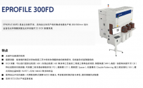
IC integrated circuit detection solution

business background

IC design (Integrated Circuit Design) is called integrated circuit design. In the nano-process technology, the fineness of integrated circuits is very high, and the higher the precision, the more advanced the production process. When more transistors are integrated in the processor, the chip can realize more functions, which directly reduces the production cost of the processor. However, as the process nodes in integrated circuits are getting smaller and smaller, the measurement of critical dimensions is also facing great challenges. How to measure and analyze geometrical information such as nanostructure period, line width, line height, sidewall angle, and roughness is extremely important. important.

solution

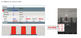
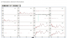
16 sets of polarization information are obtained through ME-L Muller matrix ellipsometry, and then the ellipsometric parameters (Ψ: amplitude ratio, △: phase difference) are obtained more accurately, fitted with hundreds of built-in optical models, and then measured Analyze the geometric shape information such as nanostructure period, line width, line height, side wall angle, roughness, etc.

1683657074486.png
1683657122215.png

Please, Log in or Register to view URLs content!
 

tokenanalyst

Brigadier
Registered Member

Kuaike Intelligent plans to build a semiconductor packaging equipment R & D and manufacturing project with 1 billion yuan.​


On May 9, Quake Intelligent Equipment Co., Ltd. announced that it intends to sign the "Area Entry Agreement" with the Management Committee of Wujin National High-tech Industrial Development Zone to invest in the construction of "semiconductor packaging equipment research and development and manufacturing projects". The wholly-owned subsidiary Jiangsu Kuaikexin Equipment Technology Co., Ltd. is the main body of the project implementation. The total planned investment of the project is about 1 billion yuan, of which the investment in fixed assets is not less than 500 million yuan (estimated number, there is uncertainty). The planned land area is about 68 mu, and the construction period is about 24 months.

1683661728525.png

According to reports, Kuaike Intelligent is committed to providing intelligent equipment solutions for the field of precision electronic assembly & semiconductor packaging, focusing on semiconductor packaging, new energy, smart electric vehicles, smart terminal smart wear, precision electronics (medical electronics, data communication), etc. Industry application field. Kuaike Intelligent has expanded precision welding technology and equipment automation capabilities to the field of power semiconductor packaging. The self-developed nano-silver sintering equipment has broken through the "stuck neck" technology of the third-generation semiconductor power chip packaging. This project has been recognized by the Jiangsu Provincial Department of Industry and Information Technology For key core technology (equipment) industrialization projects, with the successful development of IGBT multi-functional die-bonding machine, formic acid welding furnace and die-bonding AOI, the capability of complete solutions for power semiconductor packaging has been formed. Quick Smart will continue to develop technologies such as high-speed and high-precision control systems, and actively deploy advanced packaging and high-end equipment.

Please, Log in or Register to view URLs content!
 

paiemon

Junior Member
Registered Member
According to the prospectus, Maolai Optical’s main customers include Camtek, KLA, Onto Innovation, CYBEROPTICS, Shanghai Microelectronics, ALIGN, Thermo Fisher, Bio-Rad, MGI, Google’s parent company Alphabet’s autonomous driving platform Waymo, Microsoft, Facebook, IDEMIA, Beijing Institute of Space Mechatronics (508 Institute), etc.
This is an important item to note. It shows that the expertise and product performance has reached the level to be qualified as a supplier to tier 1 companies/institutions (both international and domestic). It shows the importance of maintaining those multinational supply chain linkages, because you improve yourself by competing against others and meeting those benchmarks. Being a supplier to those companies also allow you to learn from them as you meet their requirements, specs, etc which feed into your internal processes and drive improvements. The work they have done with their global customers translates into expertise that will support localization efforts. That's why despite all the hits from the US government, China has not prevented Chinese companies from working with their US counterparts with few exceptions because of the gains through supply chain integration and a diverse customer base. It may seem counterintuitive to allow a Chinese company to supply KLA when they are restricted from selling into China, but any localization efforts have a solid supply chain base to build from instead of having to create that expertise from scratch.
 

ansy1968

Brigadier
Registered Member
@olalavn , Sir Is Hisilicon KC10 is based on SMIC 7nm N+2 chiplets? As reported it is comparable to Qualcomm Snapdragon 8 Gen 2 being produced by TSMC using 4nm technology?

Please, Log in or Register to view URLs content!


Please, Log in or Register to view URLs content!

Please, Log in or Register to view URLs content!


Please, Log in or Register to view URLs content!

Jan 12, 2023 — Amid U.S. sanctions, a new Kirin KC10 chipset has appeared in testing Huawei Mate 50 Pro smartphone, the screenshot shows that the chip is ...

Please, Log in or Register to view URLs content!


Please, Log in or Register to view URLs content!

Please, Log in or Register to view URLs content!


Please, Log in or Register to view URLs content!

The latest Kirin KC10 SOC leaked, the performance is matching the Snapdragon 8 Gen 2,. Despite being banned by the U.S., Huawei is still testing new Kirin ...

Please, Log in or Register to view URLs content!


Please, Log in or Register to view URLs content!

Please, Log in or Register to view URLs content!


Please, Log in or Register to view URLs content!

chinesenews #6g #chinesetechnology #zte #huawei #5g #chinavsusa. ... Huawei will release the self-developed Kirin KC10 chip, ...
YouTube · Fantastic Vision · 1 hour ago

Please, Log in or Register to view URLs content!


Please, Log in or Register to view URLs content!

Please, Log in or Register to view URLs content!


Mar 14, 2023 — According to earlier rumours, Huawei might bring back the Kirin processor. ... posted a notice of a Kirin chip with the codename KC10.
Pros and cons: Significant improvements in graphics performance ⋅
Please, Log in or Register to view URLs content!
 

european_guy

Junior Member
Registered Member

Smart driving advances, the journey is shared - the shipment of Horizon Journey chips exceeds 3 million pieces​


Please, Log in or Register to view URLs content!

Their
Please, Log in or Register to view URLs content!
is a 16nm AI chip, independently developed with 128TOPS of computing power for autonomous driving.

The fact that they sold more than 3 million chips is quite a achievement. A real competitor to NVIDIA and Qualcomm in the emerging autonomous driving market....at the moment they even have been spared from the “Entity List".


Please, Log in or Register to view URLs content!
this year. Quite an achievement! For emerging Chinese NEV, the ADAS chip is the last link to be really fully independent in this new and very strategic market.

To note that (very wisely) it is has been developed on 16nm instead of sub-7nm as their US competitors. This should give them some shield from the possible US ban.
 
Last edited:

bzhong05

New Member
Registered Member
Please, Log in or Register to view URLs content!

CXMT plans to go public on Shanghai's STAR board after clearing US export controls. Company has a valuation of well over RMB 100 billion ($14.5 billion) and has planned to increase capital expenditure in 2023 by $4-5 billion. Likely to get tools from the US as company was told by suppliers that their chipmaking equipment would not be subject to export controls but is also looking at domestic suppliers as well. Chinese industry sources say CXMT is about "4 generations behind" Micron, however.
 
Status
Not open for further replies.
Top