Chinese semiconductor industry

Status
Not open for further replies.

tokenanalyst

Brigadier
Registered Member
Piotech's revenue and net profit both increased significantly last year, with sales orders in hand amounting to 4.602 billion yuan

Please, Log in or Register to view URLs content!
Tuojing Technology's SACVD products continue to improve product competitiveness and actively expand application fields. SACVD equipment that can achieve SA TEOS, BPSG, and SAF thin film process deposition has passed customer verification and realized industrial applications. At present, the company's SACVD products have been widely used in domestic integrated circuit manufacturing production lines, and have obtained orders from existing and new customers.

HDPCVD (High Density plasma) equipment can perform thin film deposition and sputtering at the same time, and the deposited thin film has higher density and lower impurity content. The HDPCVD (PF-300T Hesper) equipment developed by the company has been shipped to the client for industrialization verification. As of the disclosure date of this report, the equipment has passed the production line verification and has been sold. The company's HDPCVD (PF-300T Hesper, TS 300S Hesper) equipment has obtained orders from different customers, and can deposit SiO2, FSG, PSG and other dielectric material films.

What is HDPCVD?

HDPCVD uses an inductively coupled plasma to generate a significantly higher plasma density than that derived from more conventional parallel plate PECVD configurations. In addition, HDPCVD includes the capability to bias the substrate, a feature usually absent from PECVD. This combination encourages denser films at lower temperatures than deposited with PECVD and adds capability to assist in planarizing patterned surfaces and fill higher aspect features such as trenches and holes without creating voids.
 

tokenanalyst

Brigadier
Registered Member
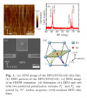
A Ferroelectric Domain-Wall Transistor
Yang-Jun Ou, Jie Sun, Yi-Ming Li, and An-Quan Jiang*​
State Key Laboratory of ASIC & System, School of Microelectronics, Fudan University, Shanghai 200433, China​

On the basis of novel properties of ferroelectric conducting domain walls, the domain wall nanoelectronics emerges and provides a brand-new dimension for the development of high-density, high-speed and energy-efficient nanodevices. For in-memory computing, three-terminal devices with both logic and memory functions such as transistors purely based on ferroelectric domain walls are urgently required. Here, a prototype ferroelectric domain-wall transistor with a well-designed coplanar electrode geometry is demonstrated on epitaxial BiFeO33 thin films. For the logic function, the current switching between on/off states of the transistor depends on the creation or elimination of conducting domain walls between drain and source electrodes. For the data storage, the transistor can maintain nonvolatile on/off states after the write/erase operations, providing an innovative approach for the development of the domain wall nanoelectronics.

1681843365566.png

Please, Log in or Register to view URLs content!
 

tokenanalyst

Brigadier
Registered Member
Lmao they propose putting suicide switch on GPU.

Tfw your GPU killed remotely because you overclock
Then a fast agile company like DJI from China or anywhere else appears, offers unrestricted AI to everyone with no bullshit no export control crap and cheap, the US AI industry lose market share and after US AI industry declines guys like this dude will start screaming "BUH MUH NATIONAL SECURITY" blaming everyone else but especially China except themselves.
 

tokenanalyst

Brigadier
Registered Member
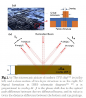
Improving on Accuracy and Sensitivity of Diffraction-based Overlay Metrology


China;Shanghai Institute of Optics and Fine Mechanics Chinese Academy of Sciences; China; China;Shanghai Institute of Optics and Fine Mechanics Chinese Academy of Sciences;Shanghai Institute of Optics and Fine Mechanics Chinese Academy of Sciences;
Shanghai Institute of Optics and Fine Mechanics Chinese Academy of Sciences;

Overlay (OVL) for pattern placed at two different layers during microchip production is a key parameter to control the manufacturing process. The tolerance of overlay metrology for the latest microchip has to be at nm scale. This paper discusses the influence on the accuracy and sensitivity of diffraction-based overlay (DBO) after developing inspection (ADI) and after etching inspection (AEI) by the asymmetric deformation of the overlay mark induced by chemical mechanical polishing (CMP) or etching. We show that the accuracy and sensitivity of DBO metrology can be improved significantly by matching the measuring light wavelength to the thickness between layers and by collecting high order diffraction signal, which is a promising solution for future overlay metrology equipment.​

1681853733534.png

Please, Log in or Register to view URLs content!
 

tokenanalyst

Brigadier
Registered Member
Thick-mask model based on multi-channel U-Net for EUV lithography

Chengzhen Yu, Xu Ma


Beijing Institute of Technology (China)

Abstract
Mask three-dimensional (M3D) effects are non-negligible for imaging simulation of EUV lithography systems. Especially, the curvilinear mask obtained by inverse lithography technique (ILT) increases the difficulty to calculate the diffraction spectrum of the thick masks. In this paper, a fast thick-mask model based on multi-channel U-Net (MCU-Net) is proposed to solve this problem. The diffraction near-field (DNF) of thick mask in EUV lithography is characterized by four complex-valued diffraction matrices, the real parts and imagery parts of which can be represented by eight realvalued diffraction matrices in total. Then, all of the eight real-valued diffraction matrices can be synthesized together using the proposed MCU-Net model. The parameters of MCU-Net are trained in a supervised manner based on a precalculated DNF dataset of curvilinear thick masks. The comparison of the proposed method with some other learningbased thick-mask models is provided and discussed. It shows that the MCU-Net is efficient and accurate to simulation the M3D effect in EUV lithography.​

Please, Log in or Register to view URLs content!
 
Status
Not open for further replies.
Top