Chinese semiconductor industry

Status
Not open for further replies.

ansy1968

Brigadier
Registered Member
continue...

The specific content of the EUV patent of Harbin Institute of Technology from 2000 to 2020​

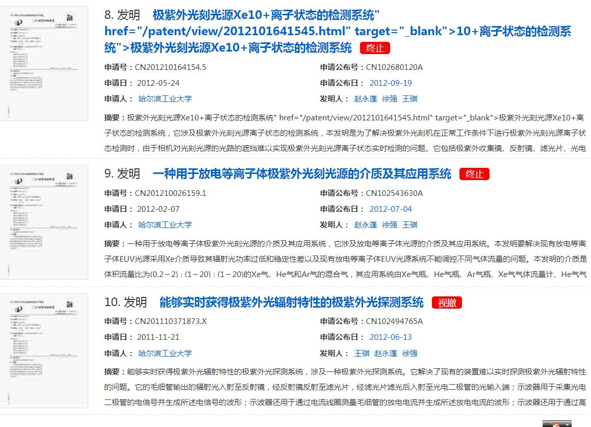
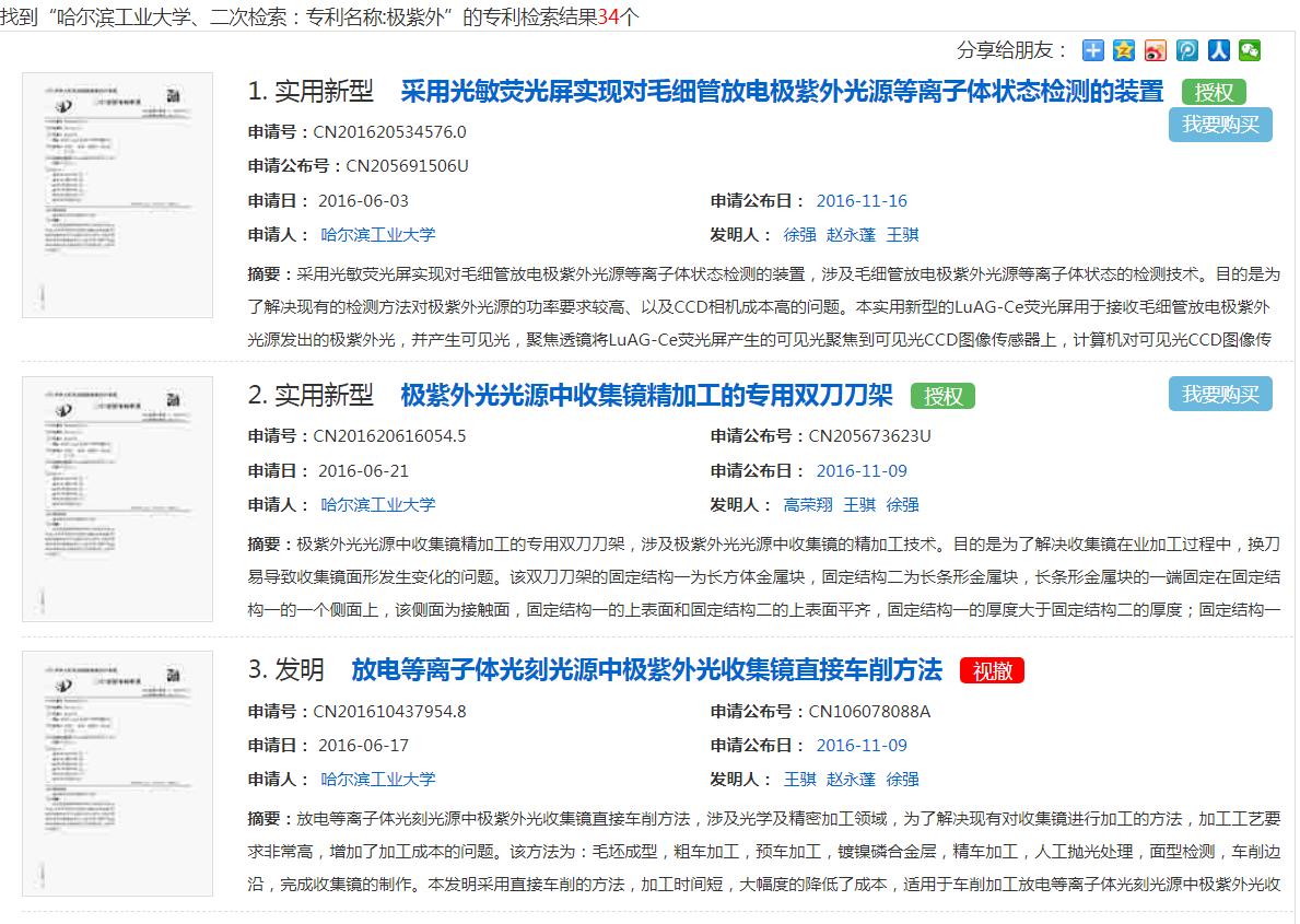
Since the English patent database contains some temporary patents, patent application documents, and patent documents, in order to more accurately analyze the content of the EUV patents of Harbin Institute of Technology, I focused on its 34 searchable patent documents in the Chinese patent database .
On the whole, in addition to some utility model patents, there are also a large number of withdrawn and terminated patent documents (Figure 6, Figure 7). Therefore , the number of effective invention patents is about 10 or so .
Interpretation of the dilemma of domestic lithography machine (9): Harbin Institute of Technology's EUV lithography machine light source


Interpretation of the dilemma of domestic lithography machine (9): Harbin Institute of Technology's EUV lithography machine light source

Some of the main invention patents are as follows:
2013-09-23:The finishing method of direct turning processing of the optical collecting mirror in the extreme ultraviolet lithography light source

2013-09-24:Invented the direct turning and rough machining method of the optical collecting mirror in the extreme ultraviolet lithography light source
2015-02-16:Invented the discharge chamber of the extreme ultraviolet light source for Xe dielectric capillary discharge detection
2016-05-31 : Invented a discharge electrode for capillary extreme ultraviolet lithography light source

2016-06-17:Invented the base for the integration of the extreme ultraviolet lithography light source to collect the lens
2016-06-20:Invented a collection system for capillary discharge Z-pinch extreme ultraviolet lithography light source
2016-06-22 : Invented a method for obtaining the circuit parameters of the magnetic pulse compression network in the power supply of the extreme ultraviolet light source

From the patent list, we can see that the EUV light source technology of Harbin Institute of Technology is actually based on the Xe gas capillary discharge technology , which is an early DPP light source technology.
It is worth mentioning that a 2016 patent " Inventing a discharge electrode for capillary extreme ultraviolet lithography light source " has been authorized by Heilongjiang Industrial Technology Research Institute (Figure 8). Whether this technology is used to manufacture DPP light sources is currently unknown.
Interpretation of the dilemma of domestic lithography machine (9): Harbin Institute of Technology's EUV lithography machine light source
 

ansy1968

Brigadier
Registered Member
continue.....

Researcher's situation​

According to the EUV patent data of Harbin Institute of Technology, all of the patents are from these four researchers:
Zhu Dongyuan , Wang Qi , Xu Qiang , Zhao Yongpeng .
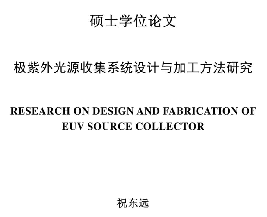
Zhu Dongyuan is a graduate student of Harbin Institute of Technology in 2012 (Figure 9). He mainly studied the simulation design of the extreme ultraviolet light source collection system and proposed a set of processing methods.

Interpretation of the dilemma of domestic lithography machine (9): Harbin Institute of Technology's EUV lithography machine light source

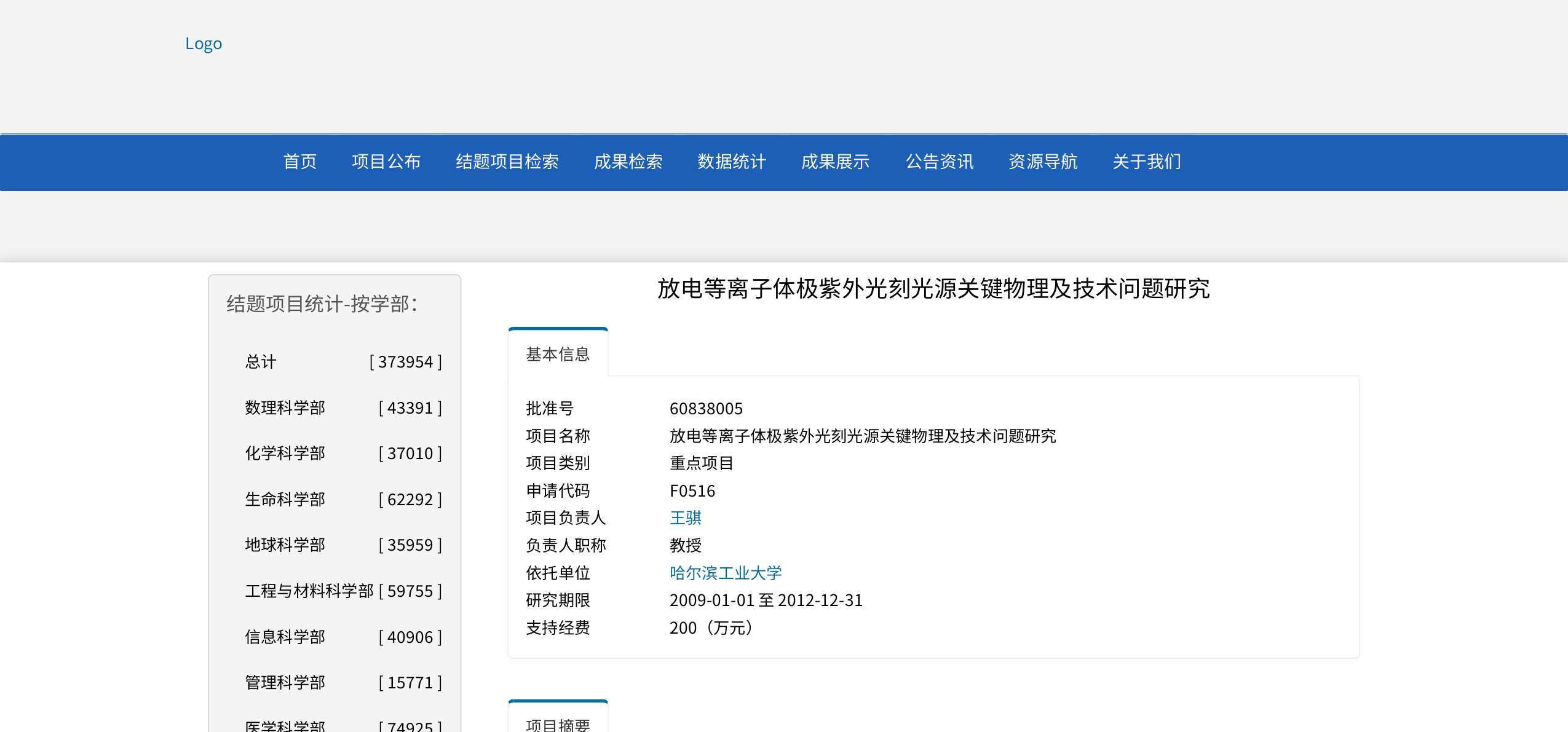
Professor Wang Qi is a doctoral supervisor of the Institute of Optoelectronic Technology, School of Astronautics , Harbin Institute of Technology, a member of the Optoelectronic Technology Expert Group of the General Armament Department, and a member of the Subject Review Group of the National Natural Science Foundation of China. He graduated from Harbin Institute of Technology with a bachelor's degree in nuclear physics in 1964. Presided over the 2009-2012 National Natural Science Foundation of China project " Research on Key Physics and Technical Issues of Discharge Plasma Extreme Ultraviolet Lithography Light Source " (Figure 10). Under the conditions of domestic technology gaps , the project developed and constructed innovative thinking The repetitive frequency 1kHz capillary discharge electrode ultraviolet lithography light source system has independently designed and developed all the unit components, breaking through the domestic related technology gap. This project can be said to have laid the foundation for the DPP research of Harbin Institute of Technology.
Interpretation of the dilemma of domestic lithography machine (9): Harbin Institute of Technology's EUV lithography machine light source


Qiang Xu graduated from Harbin Institute of Technology with a Ph.D. degree in physics and electronics in September 2014. The title of Dr. Xu Qiang's graduation thesis is " Capillary Discharge Z-pinch Xe Plasma EUV Light Source " (Figure 11), which shows that it is the main force of EUV light source research.
Interpretation of the dilemma of domestic lithography machine (9): Harbin Institute of Technology's EUV lithography machine light source

1. Xu Qiang, Tian He, Zhao Yongpeng, et al., Influence of Pre-Ionized Plasma on the Dynamics of a Tin Laser-Triggered Discharge-Plasma, Applied Sciences, 2019, 9(23), 4981

2. Xu Qiang, Deng Xiaolong, Tian He, et al., Effect of Time Delay on Laser-Triggered Discharge Plasma for a Beyond EUV Source, Symmetry, 2019, 11(5), 658
Zhao Yongpeng , a doctoral student graduated from Harbin Institute of Technology in 2001, is the deputy dean of the School of Astronautics, Harbin Institute of Technology. Since 1995, he has been engaged in the research of soft X-ray laser and extreme ultraviolet light source, and published more than 70 papers in domestic and foreign magazines. He is the leader of the EUV light source project. From the public information, Professor Zhao Yongpeng is the main person in charge of the capillary discharge DPP EUV project. However, its research direction is short-wavelength lasers. Recently, a series of papers have been published, which are various short-wavelength lasers based on the principle of capillary discharge. Their expertise is not in EUV light sources. Professor Yongpeng Zhao is also the supervisor of Dr. Qiang Xu.
 

ansy1968

Brigadier
Registered Member
Last part.....


Harbin Institute of Technology EUV Research Direction​

At the beginning of this article, we mentioned that there are three main EUV technologies: the first-generation DPP discharge technology, the second-generation LDP technology, and the third-generation LPP technology . The Harbin Institute of Technology concentrated research on the earliest first-generation DPP technology based on capillary discharge .

The development history of the capillary discharge electrode UV light source is roughly as follows:
1988: Rocca, a scholar at Colorado State University in the United States, first proposed the idea of a desktop laser that uses capillary discharge to generate soft X-rays or extreme ultraviolet lasers.
1994: The Rocca group realized the first time that a capillary discharge neon-like chlorine generates a 46.9 nm laser

1997:
The research group of American scholar Klosner used LiH capillary discharge to obtain a soft X-ray output of 13.5 nm
1998: The
Klosner research group observed a higher intensity 10-16 nm soft X-ray output during the capillary discharge process filled with Xe , achieving a technological breakthrough.
In other words, Harbin Institute of Technology actually mastered the DPP technology of the Klosner research group in the United States in 1998 .

Harbin Institute of Technology EUV Research Results​

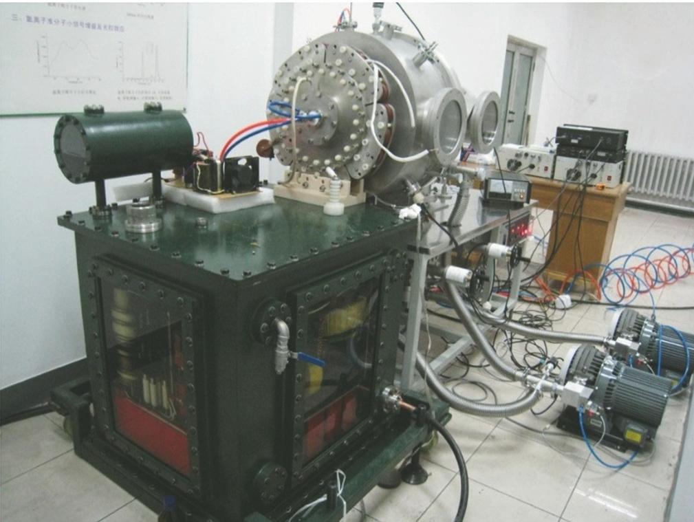
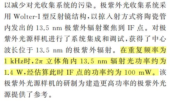
In December 2018, Professor Zhao Yongpeng of Harbin Institute of Technology published a review article (Figure 1), describing the work of Harbin Institute of Technology on the 13.5nm discharge Xe plasma extreme ultraviolet light source. The article shows the latest prototype of the discharge Xe plasma extreme ultraviolet light source with a repetition frequency of 1 kHz (Figure 13) .
Interpretation of the dilemma of domestic lithography machine (9): Harbin Institute of Technology's EUV lithography machine light source

Interpretation of the dilemma of domestic lithography machine (9): Harbin Institute of Technology's EUV lithography machine light source


Going back to the voting link mentioned at the beginning of this article, here we can give the power of the EUV light source of Harbin Institute of Technology. Please see Figure 14 for the numbers. friends? Is this number the same as your estimate?
Interpretation of the dilemma of domestic lithography machine (9): Harbin Institute of Technology's EUV lithography machine light source

Concluding remarks​

Harbin Institute of Technology has a good foundation for EUV research in the early stage. Professor Wang Qi's doctoral student, Zhang Xingqiang, wrote his PhD thesis in 2008 on "Capillary Discharge X-ray Laser Characteristics and UV Lithography Source Research". At this time, it was only 10 years since the United States invented the Xe plasma discharge DPP technology, and it was only 5 years since the first 35-watt light source launched by Xtreme in 2003 .
However, it is a pity that while Europe, the United States and Japan are vigorously carrying out LDP and LPP research, China seldom takes any action. And in the 02 project, the most backward Xe gas plasma DPP technology was still used as a research topic , and the technology to catch up was lost. Even in terms of DPP and LDP technologies that have been temporarily eliminated by the market, China's basic research is still very different. During this period, I discovered that Li Xiaoqiang, a 2014 graduate student at Harbin Institute of Technology, did some research on the 13.5 nm extreme ultraviolet radiation of laser-assisted discharge Sn plasma, but there was no follow-up work.
What's even more regrettable is that we have not seen that generation after generation of students graduated from Harbin Institute of Technology can stick to EUV technology. Of course, this is related to the objective laws of technological development. We can't blame a few professors and doctors in universities for being able to complete the great industrialization that can be accomplished by investing billions, tens of billions, and dozens of top lithography machine manufacturing teams from abroad. . The publicly reported DPP light source that has been completed so far is only at the level of the 1998 study in the United States .
We have been talking about Harbin Institute of Technology from Changchun Institute of Optics and Mechanics, Huazhong University of Science and Technology, and Shanghai Institute of Optics and Mechanics . In fact, I believe that most of my friends should have realized the overall research status and reality of domestic universities. We are not terribly bad, but we also don't have very good strength and technical reserves that the outside world imagines. On the contrary, we see that most of the technology only stays at the time node of 2000-2005 , that is to say, we do not have any organization and ability to carry out the industrialization of EUV lithography machines.
At this point, I think my friends should have a more comprehensive understanding of the research status of domestic EUV light sources, right?
See you next time
 

FairAndUnbiased

Brigadier
Registered Member
I've been getting that sense as well. I'm eager to see what becomes of it and how well the machine performs.

Japan's and Dutch DUV offerings are extremely advanced. They are also very profitable machines, from what I understand. Don't forget, that this is all a far-cry from EUV as well. ASML is already on their 2nd gen EUV machine. We'll see how fast China can catch up.
only Dutch. Japanese DUV is on life support as Intel moves into EUV for critical layers and uses their old Nikons for metal layers. I suspect use of Nikon was the reason they had issues pre-EUV post multipatterning, as Nikon ArF immersion tools don't have dual stage for in situ metrology. Nikon declined to 7% market share from ~40% or something in their heyday 15-30 years ago.

Please, Log in or Register to view URLs content!
 

FairAndUnbiased

Brigadier
Registered Member
Well that depends on how long it'll take China to develop and mass produce an EUV machine. SMEE's 28 nm machine is still not in mass production, or am I wrong?
EUV core tech is entirely independent from ArF immersion core tech. Even for wafer stage, EUV uses maglev stage while ArF uses air stage so the drive mechanism, control mechanism, etc are totally different. EUV cannot use air stage because it must be moved in a vacuum.

The key limitation of EUV is the light source being powerful enough and the ultrahigh vacuum environment required - both of which have nothing to do with ArF. In some aspects, EUV has some elegant simplicity:

1. ArF immersion requires management of a complex and moving lens-liquid-photoresist interface. EUV has only a simple vacuum-photoresist interface.

2. ArF uses complex refractive optical elements that require 3D precision machining and polishing which requires lots of experience in lenscrafting from the old industrial era. Note that this is not machining and polishing of glass, but of exotic UV transparent materials like CaF2.

EUV uses reflective optics that are made with multilayer vapor deposition techniques on a smooth substrate (like a simple wafer). Large area precision PVD up to 300 mm size (on a standard 300 mm wafer) and with nm level precision is a solved problem in China, proven by the fact that fabs work and all fabs use metal PVD.

Please, Log in or Register to view URLs content!

3. No need for multipatterning, just single pattern and done for 14 nm and 7 nm. 5 nm will require double patterning with EUV, and at that point we start hitting diminishing returns anyhow.

Please, Log in or Register to view URLs content!
 
Last edited:

ansy1968

Brigadier
Registered Member
I suppose that with Harbin Institute of Technology out of the running, the work falls to CETC and Huawei. Rather disappointing, but given the apparent neglect and researchers leaving behind an older technology isn't completely surprising.
No bro HIT is one of many Scientific institution working on EUV, they may hit a road block BUT success is a product of many failures. In fact they're the one who introduced a PLANAR Grating inferometer that enable the success of SSA800 DUVL.

China is working on 4 different type of power source, it may seem wasteful BUT necessity is the mother of invention. There is a division of work with HIT focusing on DPP & LPD, CIOMP on LPP while CAS on SSMB, they're covering all bases possible to have a breakthrough.
 
Last edited:

tphuang

Lieutenant General
Staff member
Super Moderator
VIP Professional
Registered Member
Please, Log in or Register to view URLs content!
2月17日,高性能嵌入式解决方案领导厂商上海先楫半导体(HPMicro)宣布,推出全新的通用微控制器(MCU) HPM6200系列,主要面向工业和汽车领域,拥有超强的CPU性能、创新的实时控制外设、工业和车规级的品质。

据悉,先楫HPM6200系列基于团队多年的产品和应用经验积累,从IP设计、架构到软件,都经过了深度优化,是一款拥有完全自主产权的高性能MCU产品。

它有望打破国外大厂在新能源、储能等领域筑起的高壁垒,真正解决卡脖子的问题。
HPMicro announces HPM6200 series of MCUs for industrial and automotive sectors. Everything is self developed according to HPMicro. Not sure who is producing it, but probably SMIC or Huahong.
HPM6200系列共有12产品型号,均基于开放的RISC-V指令集架构,可选单核、双核,可选144 LQFP、116 BGA两种封装(与已量产的HPM6300系列兼容),可选内置4MB闪存或无闪存,全线通过AEC-Q100认证,工作温度范围从零下40℃到125℃。

其中,双核型号主频达到600MHz,支持双精度浮点运算、强大DSP扩展,性能达到6780 CoreMark、3420 DMIPS,可在1微秒内完成基于矢量控制的电流控制环路运算。
Looks like this is quite capable and can be used in wide range of field and environment.

RISC-V seems to be the future for MCUs.
 

tokenanalyst

Brigadier
Registered Member

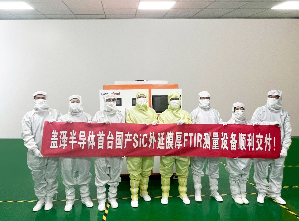
Breaking the monopoly, GEZE Semiconductor successfully delivered the first domestic SiC epitaxial film thickness measurement equipment!​


The cyclicality of semiconductor equipment is weakening in recent years, and the industry growth trend is strengthening. According to data from the International Semiconductor Industry Association (SEMI), total sales of semiconductor manufacturing equipment are expected to reach a new high of US$108.5 billion in 2022, an increase of 5.9% from the industry record of US$102.5 billion in 2021. Among them, the semiconductor test equipment market sales are expected to be US$7.6 billion in 2022. In the semiconductor manufacturing link measurement equipment market, foreign companies such as Kelei, Applied Materials, and Hitachi High-Tech have formed a giant monopoly advantage, and the localization rate is extremely low. In the segmented field, FTIR wafer measurement equipment also mostly relies on imports from foreign manufacturers.

As an early local enterprise in the field of semiconductor equipment, Huasi Gaize Semiconductor Technology (Shanghai) Co., Ltd. (referred to as " Gaiza Semiconductor ") provides high-precision optical inspection equipment for wafer products. At present, the SiC epitaxial film thickness measurement equipment GS-M06Y independently developed and produced has been officially delivered to customers .

790206603602.57951311753346913.563.png


GS-M06Y will be applied to semiconductor front-end measurement, mainly for silicon epitaxial/silicon carbide epitaxial layer thickness measurement. The GS-M06Y equipment adopts the high-precision algorithm, Load Port, control software and FTIR optical system independently developed by GEZE Semiconductor. The FTIR optical path system independently developed by the company can quickly detect the thickness of the wafer, and realize the requirements of fast scanning speed, high resolution and high sensitivity.

It is worth mentioning that compared with the same type of products from foreign competitors, GEZE Semiconductor testing equipment has the following two advantages:

Strong compatibility, can be customized based on customer needs.
At present, the domestic market of FTIR Fourier transform infrared wafer measurement equipment relies heavily on imports, and most of the imported equipment are preset programs with low compatibility and cannot be customized for domestic enterprises. GEZE semiconductor testing equipment can meet the different needs of customers, and customize equipment according to customer requirements, such as docking with customer MES systems or improving software according to engineer habits, which can greatly reduce customer use and maintenance costs.

The measurement time is shorter and the accuracy is higher. GS-M06Y has reached the international leading level in the performance of measuring silicon wafer speed, single-chip silicon wafer measuring time, measurement accuracy, test repeatability, and single-point repeatability, and some performances even surpass similar foreign products.

According to Jiwei.com, the equipment shipped this time is different from the previous ones. This equipment uses the latest silicon carbide epitaxy detection technology developed by Gaize Semiconductor, which can accurately measure the silicon carbide epitaxy. After the equipment is shipped, another milestone for the company. GEZE Semiconductor not only breaks through the SiC epitaxial detection technology, but also realizes the first-generation semiconductor (silicon epitaxy 6 inches & 8 inches & 12 inches), the second-generation semiconductor (gallium arsenide, indium phosphide substrate epitaxy 4 inches & 6 inches & 8 inches), the third-generation semiconductor Semiconductor (silicon carbide epitaxy 4 inches & 6 inches & 8 inches, gallium nitride epitaxy), SOI wafer top layer silicon 6 inches & 8 inches & 12 inches, and different epitaxial layer thickness measurements in the silicon germanium epitaxy process.

Please, Log in or Register to view URLs content!
 

latenlazy

Brigadier

Harbin Institute of Technology EUV Research Direction​

At the beginning of this article, we mentioned that there are three main EUV technologies: the first-generation DPP discharge technology, the second-generation LDP technology, and the third-generation LPP technology . The Harbin Institute of Technology concentrated research on the earliest first-generation DPP technology based on capillary discharge .

The development history of the capillary discharge electrode UV light source is roughly as follows:
1988: Rocca, a scholar at Colorado State University in the United States, first proposed the idea of a desktop laser that uses capillary discharge to generate soft X-rays or extreme ultraviolet lasers.
1994: The Rocca group realized the first time that a capillary discharge neon-like chlorine generates a 46.9 nm laser

1997:
The research group of American scholar Klosner used LiH capillary discharge to obtain a soft X-ray output of 13.5 nm
1998: The
Klosner research group observed a higher intensity 10-16 nm soft X-ray output during the capillary discharge process filled with Xe , achieving a technological breakthrough.
In other words, Harbin Institute of Technology actually mastered the DPP technology of the Klosner research group in the United States in 1998 .

Harbin Institute of Technology EUV Research Results​

In December 2018, Professor Zhao Yongpeng of Harbin Institute of Technology published a review article (Figure 1), describing the work of Harbin Institute of Technology on the 13.5nm discharge Xe plasma extreme ultraviolet light source. The article shows the latest prototype of the discharge Xe plasma extreme ultraviolet light source with a repetition frequency of 1 kHz (Figure 13) .
Interpretation of the dilemma of domestic lithography machine (9): Harbin Institute of Technology's EUV lithography machine light source's EUV lithography machine light source

Interpretation of the dilemma of domestic lithography machine (9): Harbin Institute of Technology's EUV lithography machine light source's EUV lithography machine light source


Going back to the voting link mentioned at the beginning of this article, here we can give the power of the EUV light source of Harbin Institute of Technology. Please see Figure 14 for the numbers. friends? Is this number the same as your estimate?
Interpretation of the dilemma of domestic lithography machine (9): Harbin Institute of Technology's EUV lithography machine light source's EUV lithography machine light source

Concluding remarks​

Harbin Institute of Technology has a good foundation for EUV research in the early stage. Professor Wang Qi's doctoral student, Zhang Xingqiang, wrote his PhD thesis in 2008 on "Capillary Discharge X-ray Laser Characteristics and UV Lithography Source Research". At this time, it was only 10 years since the United States invented the Xe plasma discharge DPP technology, and it was only 5 years since the first 35-watt light source launched by Xtreme in 2003 .
However, it is a pity that while Europe, the United States and Japan are vigorously carrying out LDP and LPP research, China seldom takes any action. And in the 02 project, the most backward Xe gas plasma DPP technology was still used as a research topic , and the technology to catch up was lost. Even in terms of DPP and LDP technologies that have been temporarily eliminated by the market, China's basic research is still very different. During this period, I discovered that Li Xiaoqiang, a 2014 graduate student at Harbin Institute of Technology, did some research on the 13.5 nm extreme ultraviolet radiation of laser-assisted discharge Sn plasma, but there was no follow-up work.
What's even more regrettable is that we have not seen that generation after generation of students graduated from Harbin Institute of Technology can stick to EUV technology. Of course, this is related to the objective laws of technological development. We can't blame a few professors and doctors in universities for being able to complete the great industrialization that can be accomplished by investing billions, tens of billions, and dozens of top lithography machine manufacturing teams from abroad. . The publicly reported DPP light source that has been completed so far is only at the level of the 1998 study in the United States .
We have been talking about Harbin Institute of Technology from Changchun Institute of Optics and Mechanics, Huazhong University of Science and Technology, and Shanghai Institute of Optics and Mechanics . In fact, I believe that most of my friends should have realized the overall research status and reality of domestic universities. We are not terribly bad, but we also don't have very good strength and technical reserves that the outside world imagines. On the contrary, we see that most of the technology only stays at the time node of 2000-2005 , that is to say, we do not have any organization and ability to carry out the industrialization of EUV lithography machines.
At this point, I think my friends should have a more comprehensive understanding of the research status of domestic EUV light sources, right?
See you next time
This is decent fact finding followed with bad interpretative work. For one, this person makes a very big leap assuming that Harbin’s DPP source was only at the level of a demonstrator technology from 1998 based on matching Xe discharge frequency. If he understood the technology he was talking about he’d probably realize that the determinant of power output for the source isn’t going to be discharge frequency of the source gas but from *quantity* of source gas and *power* of the Z pinch that can be formed by the electrode. That doesn’t mean the technology wasn’t a dead end but it does mean he has no basis to conclude that they were only perfecting capabilities that were more than two decades old.

Second, he assumes that if the technology itself was a dead end nothing else useful came out of working on the technology. But being able to produce a light source also means enabling research for other aspects of EUV lithography outside the light source, and it seems that’s in fact exactly what this Xe gas based light source did for HIT.

Third, and this is his biggest faux pas, if the dude had just done more browsing around instead of committing to snap judgments based on one single research tree he’d have found that LPP and LDP were both also being researched during the same timespan that DPP was.

Please, Log in or Register to view URLs content!

Please, Log in or Register to view URLs content!

The Chinese blogosphere is filled with people who like to present themselves as fact checkers for the rest of the community but they often don’t know enough about the thing they’re fact checking to draw sound conclusions and need to be fact checked themselves. Pointing to credible data isn’t the same thing as finding truth.
 
Status
Not open for further replies.
Top