Chinese semiconductor industry

Status
Not open for further replies.

tphuang

Lieutenant General
Staff member
Super Moderator
VIP Professional
Registered Member
Please, Log in or Register to view URLs content!
公司是AMD最大的封装测试供应商,占其订单总数的80%以上,未来随着大客户资源整合渐入佳境,产生的协同效应将带动整个产业链持续受益
Nantong Fujitsu Micro is responsible for packaging & testing of 80% of AMD's chiplet.
Looks like they started this relationship in 2016.
 

FairAndUnbiased

Brigadier
Registered Member

tokenanalyst

Brigadier
Registered Member

The research and development and packaging project of Xinhao Semiconductor's silicon carbide devices and modules signed a contract with Lishui.​


On the afternoon of February 14th, Lishui City held a signing ceremony for the revitalization and development of the old revolutionary base area and the major project of double recruitment and double introduction. 89 major projects were signed, with a total investment of 120.529 billion yuan. Among them, 4 projects will be settled in Liandu, including R&D and packaging projects of silicon carbide devices and modules.

1676559449847.png


According to reports, the R&D and packaging projects of silicon carbide devices and modules are invested and constructed by Zhejiang Xinhao Semiconductor Co., Ltd. with a total investment of 1.5 billion yuan, mainly for the construction of silicon carbide device production lines and silicon carbide power module production lines. After completion, the annual output value of the project is expected to be 1.2 billion yuan.
 

tokenanalyst

Brigadier
Registered Member
Shanghai Institute of Optics and Mechanics has made progress in the detection of extreme ultraviolet lithography mask defects

  Recently, the Information Optics and Optoelectronics Technology Laboratory of Shanghai Institute of Optics and Fine Mechanics, Chinese Academy of Sciences proposed a phase defect detection technology for extreme ultraviolet (EUV) lithography masks based on generative confrontation network (GAN). Characterization using generative adversarial networks for extreme ultraviolet lithography" was published on Applied Optics .

  Multilayer film defects refer to the multilayer film deformation caused by the protrusions, depressions on the EUV lithography mask substrate and the particles falling on it during the deposition process, which will affect the amplitude and phase of the mask reflected light at the same time. Due to the short exposure wavelength of EUV lithography, only nanometer-sized multilayer film defects can cause significant phase changes in reflected light and reduce imaging quality. In order to realize mask defect compensation and repair, accurate detection of such defects is required.

  The surface topography of multilayer film defects can be measured by existing inspection equipment, such as atomic force microscope, but only measuring the surface topography is difficult to meet the needs of defect simulation analysis and accurate compensation. The three-dimensional morphology of multilayer film defects is difficult to measure directly with non-destructive measurement methods. In response to this problem, the research team proposed a phase-type defect detection technology for extreme ultraviolet lithography masks based on generative adversarial networks, which can reconstruct the three-dimensional shape of mask defects from the aerial image of mask defects. By adjusting the light angle, multiple groups of mask aerial images are taken. The spatial images of mask defects at different illumination angles are mapped to defect morphology parameters by using the expanded residual network (DRN), and a series of GANs are used to assist the learning of the defect representation model. In addition, the spatial image information of EUV lithography under different illumination angles is considered, so that the obtained defect morphology parameters are more suitable for the simulation of defect optical effects, and more in line with the requirements of accurate compensation. The simulation results with rigorous electromagnetic field simulation tools show that the method can reconstruct the three-dimensional morphology parameters of phase defects in EUV lithography masks with high precision.

1676562169564.png
Please, Log in or Register to view URLs content!
 

tokenanalyst

Brigadier
Registered Member
GAA transistor manufacturing process using ALD tools and Naura etching tools.

A Novel Si Nanosheet Channel Release Process for the Fabrication of Gate-All-Around Transistors and Its Mechanism Investigation.

Abstract​

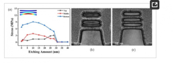
The effect of the source/drain compressive stress on the mechanical stability of stacked Si nanosheets (NS) during the process of channel release has been investigated. The stress of the nanosheets in the stacking direction increased first and then decreased during the process of channel release by technology computer-aided design (TCAD) simulation. The finite element simulation showed that the stress caused serious deformation of the nanosheets, which was also confirmed by the experiment. This study proposed a novel channel release process that utilized multi-step etching to remove the sacrificial SiGe layers instead of conventional single-step etching. By gradually releasing the stress of the SiGe layer on the nanosheets, the stress difference in the stacking direction before and after the last step of etching was significantly reduced, thus achieving equally spaced stacked nanosheets. In addition, the plasma-free oxidation treatment was introduced in the multi-step etching process to realize an outstanding selectivity of 168:1 for Si0.7Ge0.3 versus Si. The proposed novel process could realize the channel release of nanosheets with a multi-width from 30 nm to 80 nm with little Si loss, unlocking the full potential of gate-all-around (GAA) technology for digital, analog, and radio-frequency (RF) circuit applications.

2. Materials and Methods​

The main fabrication process flow of vertically stacked horizontal nanosheets is shown in Figure 1a. First, three cycles of the Si/SiGe multilayer were deposited on an eight-inch Si substrate using a reduced pressure chemical vapor deposition (RPCVD) apparatus, where the thickness of the Si and SiGe layers was around 9 nm, and the Ge composition in the SiGe layers was 30% (the Si/SiGe multilayer wafer used in this paper was a commercially available wafer). Then, a hard mask was grown on the Si/SiGe multilayer, and the designed test pattern was transferred to the hard mask. The designed test pattern was transferred to the Si/SiGe multilayer structure by anisotropic etching using the inductively coupled plasma (ICP) machine. Next, the hard mask was removed by wet etching using a 1% hydrofluoric acid solution, while the native oxide was removed. After that, the sacrificial SiGe layers of the channel were removed by isotropic etching, using the remote plasma dry etching apparatus (NAURA HSE200C) to form the suspended vertically stacked Si nanosheets. Finally, the high K dielectric and metal gate (HKMG) were uniformly wrapped on the nanosheets by atomic layer deposition (ALD) technology. The cross-section of the channel was analyzed by a high-resolution transmission electron microscope (TEM) to check the mechanical stability of the stacked nanosheets.
1676563335823.png


Please, Log in or Register to view URLs content!
 

BoraTas

Major
Registered Member
I heard that an ex-ASML employee "brought" a lot of ASML data to China. The data includes lithography data and Teamcenter files. Teamcenter is a PLM software BTW.

PLM: "PLM software is a solution that manages all of the information and processes at every step of a product or service lifecycle across globalized supply chains. This includes the data from items, parts, products, documents, requirements, engineering change orders, and quality workflows."
 

Maikeru

Major
Registered Member
I heard that an ex-ASML employee "brought" a lot of ASML data to China. The data includes lithography data and Teamcenter files. Teamcenter is a PLM software BTW.

PLM: "PLM software is a solution that manages all of the information and processes at every step of a product or service lifecycle across globalized supply chains. This includes the data from items, parts, products, documents, requirements, engineering change orders, and quality workflows."
Please, Log in or Register to view URLs content!
 

tokenanalyst

Brigadier
Registered Member
Please, Log in or Register to view URLs content!
I don't think is a big deal for ASML, probably is just generic data. They could have bigger problems if the Chinese goverment decide not to enforce the extensive ASML EUV patent portfolio in China, which they use to gatekeep every other company out of the EUV market given the fact that ASML is not allowed to sell their EUV tools in China. They even stated something like that in their reports.

ASML can't count on the idea that China will take X amount of time to develop their own EUVL tools also given the fact that they had almost two decades of experience developing EUV related technologies and breakthroughs, believe or not, can happen sooner than most people expect when there is economic pressure.

ASML best weapon to keep their monopolistic position is to sell were the competition, present and future, exist. They get to outcompete everyone, they get to make friends, process are designed exclusive for their tools and the get to enforce their extensive IP portfolio in a more efficient way.​
 
Status
Not open for further replies.
Top