Chinese semiconductor industry

Status
Not open for further replies.

sunnymaxi

Major
Registered Member
Damn, that really is impressive.

Look at the timeline of Huawei sanctions, which were 2019. So these guys at SMEE had to start working on this project on 2020 will some urgency. But the pandemic hit, which probably is another 6 month delay.

2019 Huawei sanctions. Then need time to do all preparatory work for domestic components and blueprints design, probably a year. Then to make the machine, first time trying probably a year. Add in the pandemic, 2020, 2021, blueprints, assembly, 2022 delays from pandemic, man, this is freaking fast!
indeed. especially last two years were really impressive for SMEE. they solved all the technical issues.

and look at their team. 600 top engineers working on DUVi project. more than I was expecting. its hugee

now more advance variants will come. capable to fab 14nm/7nm.
 

tokenanalyst

Brigadier
Registered Member

Heyan Technology won the second phase of investment from the National Fund to focus on semiconductor grinding equipment​

On December 29, 2022, Heyan Technology was invested by the National Integrated Circuit Industry Investment Fund Phase II Co., Ltd. (National Large Fund Phase II).

It is reported that this round of financing is the B+ round of financing of Heyan Technology, and the industrial and commercial change registration has been completed.

Established in 2011, Heyan Technology is a company specializing in the research and development, sales, consulting and service of semiconductor grinding equipment, focusing on silicon wafers, glass, ceramics, quartz, lithium niobate, silicon carbide, resin and other hard Precision cutting of brittle materials.

The company's main business is 6~12 inches DS series precision dicing machine, JS series automatic cutting and sorting machine and other semiconductor-specific precision cutting equipment, which are widely used in the manufacturing fields of integrated circuits, discrete devices, optoelectronic devices and sensitive components.

Chemical Mechanical Polishing (CMP) is a key process to achieve global planarization of wafers. The CMP process runs through silicon wafer manufacturing, integrated circuit manufacturing, packaging and testing. Polishing fluid and polishing pads are the core consumables of the CMP process, accounting for more than 80% of the CMP material market. The CMP materials and equipment companies represented by Dinglong and Huahai Qingke have attracted the attention of the industry.

The target is the core raw material for the preparation of functional thin films. It is mainly used in semiconductors, panels, photovoltaics and other fields to achieve functions such as conduction or barrier. Among the major semiconductor materials, the target is the one with the highest degree of localization. Breakthroughs have been made in the field of domestic aluminum, copper, molybdenum and other target materials. The main listed companies include Jiangfeng Electronics, Youyan New Materials, Ashichuang, Longhua Technology, etc.

The next three years will be a period of rapid development of China's semiconductor manufacturing industry. Enterprises such as SMIC, Huahong Grace, Yangtze Memory, Changxin Storage, and Silan Micro will accelerate production expansion. Geke Micro, Dingtai Jiangxin, and China Resources Micro The 12-inch wafer production line deployed by the company will also be put into production one after another, which will bring huge demand for CMP materials and targets.

Under the new situation, the security of the supply chain of domestic fabs is becoming more and more important, and it is imperative to cultivate stable local material suppliers, which will also bring huge opportunities to domestic suppliers. The successful experience of target materials will also provide reference for the localization development of other materials.

Please, Log in or Register to view URLs content!
 

pbd456

Junior Member
Registered Member
I don't know if you read Chinese or not,but that's not the meaning of his word

ID "秦声楚舞" asks:不是说接近交付吗? Translation: Didn't you say near delivery?

ID "havok" replies : 官宣交付呗,judging from the context,he is saying "just wait for official announcement about delivery"


Remember,there are some posts in the middle got deleted by havok,don't know why he did that. For instance,this post was deleted by him,so you cannot find it now

https://www.sinodefenceforum.com/attachments/%E7%81%AB%E7%8B%90%E6%88%AA%E5%9B%BE_2023-01-02t09-35-21-338z-png.104227/
The optics, the light source are not currently being mass produced right?
 

tokenanalyst

Brigadier
Registered Member

Laser Assisted Bonding Packaging Technology Introduction​


This article is about the laser-assisted bonding technology developed and mass-produced by JCET. This technology is designed to solve the problem of coreless substrate materials in the automotive field, especially in the development of packaging technologies related to electric vehicles and autonomous driving with high reliability standards. and process FCBGA products. Because the product is very thin, ordinary reflow soldering bonding technology can no longer meet the demand. In order to solve problems such as BUMP Bridge and poor contact caused by substrate warping, Changdian has developed a new interconnection technology - Laser Assisted Bonding (LAB), which has been applied to mass production, and what is even more commendable is The output of the technology's R&D investment has already contributed significantly to the company's revenue and profit growth in 2021, and will continue to achieve significant results in the company's future performance growth.

Founded in 1972, JCET is a world-leading integrated circuit manufacturing and technical service company with more than 3,200 patents. JCET has six production bases and two R&D centers in China, South Korea and Singapore, with more than 23,000 employees all over the world. JCET ranks third among the world's top ten packaging foundries and ranks first in mainland China. It is a veritable high-tech enterprise with a global vision.

So what is LAB (Laser Assisted Bonding) technology? LAB technology refers to irradiating the laser beam on the core chip or the device that needs to be welded to make the core chip and the device rise from room temperature to the welding temperature within a few seconds, and then weld it on the substrate, interposer or another core chip stacked. The whole LAB system consists of four parts: high-power diode laser source, optical fiber, collimator, and homogenizer to generate flat-top laser beam. The laser source works in continuous wave mode, using a near-infrared wavelength of 980nm, with a maximum power of 2kW, a beam size of 9 to 45mm, and a focal length of 240mm. The specific schematic diagram is shown in Figure 1.

7ca6be355dfacc0fbe8e61a32aa91587.png!a


Figure 1: Schematic Laser Source: laser source; Optical Fiber: optical fiber; Collimator: collimator; Homogenizer: homogenizer; Focal Distance: focal length; Laser Beam: laser beam

In the whole process, the power density distribution and spatial characteristics of the laser beam are extremely important. As shown in Figure 2 below, if the power distribution is uneven, it will lead to uneven temperature, resulting in BUMP bridging or poor contact defects. In some areas, due to insufficient power irradiation, it will lead to poor contact defects caused by insufficient welding temperature. In another part of the area, due to receiving too high power irradiation, there will be defects of BUMP bridging. In some extreme cases, it may even burn out the die or the device. Therefore, the difficulty of the whole process is how to evenly heat the parts to be welded. Of course, even heating in the C4/DIE BUMP area is also the advantage of the LAB process over the reflow soldering process.

54c76aa23f58c41dbf0bbeff66cc9e7c.png!a


Figure 2 Schematic diagram of LAB process defect generation


Since energy stability and controllability are so important, we can continue to discuss what level the current industry can achieve. Figure 3 and Figure 4 are the experimental data published in JCET’s article. According to the figures in the figure, we can see that the uniformity is very good, and the energy difference in the chip welding area in the lower right corner is very small.

94dbdbda5ff4489964d383da26a14ec3.png!a


Figure 3. The energy density distribution diagram in the LAB process. Each value represents the simulated value measured on a single pixel.


3c45e4c1945946452a070574c7cbd1db.png!a


Fig. 4 Distribution of energy density in XY and Z directions in LAB processing technology
 

tokenanalyst

Brigadier
Registered Member

With a registered capital of 10 million yuan, Jingsheng Electromechanical established a semiconductor equipment company in Zhejiang​


1311317560324.8108223182333592.7585.png


Jiweiwang news (text/Bai Yuxuan) Tianyan Check shows that recently, Zhejiang Jingsheng Chuangxin Semiconductor Equipment Co., Ltd. was established. The legal representative is Cao Jianwei, with a registered capital of 10 million yuan. The business scope includes: manufacturing of special equipment for semiconductor devices; Sales of special equipment for devices; manufacturing of special electronic equipment; sales of special electronic equipment; technical services, technical development, technical consultation, technical exchanges, technology transfer, technology promotion; technology import and export; goods import and export; mechanical parts, parts processing; mechanical parts , Parts sales.

Please, Log in or Register to view URLs content!
 

tphuang

Lieutenant General
Staff member
Super Moderator
VIP Professional
Registered Member

european_guy

Junior Member
Registered Member

FairAndUnbiased

Brigadier
Registered Member
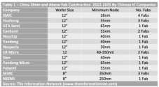
The planned fab expansions in China equate to 1,334kwpm which will almost double the current wafer capacity (1,665kwpm) and add 6% to the global wafer capacity.
View attachment 104336
View attachment 104337
Please, Log in or Register to view URLs content!
Wonder what the applications of the mid tier wafers (32-90 nm) will be. MCUs, power, analog, etc. can be done with super cheap KrF tools at 130+ nm. Once you get to <90 nm you have to use dry ArF, a step up in cost. From that list I see lots of automotive chip companies like CanSEMI and CR Micro.
 
Status
Not open for further replies.
Top