You are using an out of date browser. It may not display this or other websites correctly.
You should upgrade or use an alternative browser.
You should upgrade or use an alternative browser.
Chinese semiconductor industry
- Thread starter Hendrik_2000
- Start date
- Status
- Not open for further replies.
This is the last chance for the US to block all possible ways for China to grow its semicon enterprises.Interesting thread. Not sure how reliable Paul Triolo is?
Another article:
Fortunately China has accumulated enough equipment to last for at least 2-3 years which is sufficient to develop new and improved domestic equipment by 2024/5. Furthermore, there was a mention on twitter by a guy Shank Hu that China now has its own tech to make <5nm chips. We shall see in 3 yrs time, max.
Wow, I can't believe its been 18 months since I wrote that article. on Applied and Lam on NAND.I already suspect so.
But from his writing, I can see his clear argument that the YMTC dependency on several (or maybe just one) tool/equipment from overseas is the achilles heel and the reason why the ban will drag YMTC. I am not saying he must be right.
Thats why I am interested to hear from some expert here how wrong he is, and the comparable alternative from domestic for the tools/equipments.
Btw, this is the information from year 2020:
Applied Materials and Lam Research generated an estimated $6.2 billion in revenues from NAND manufacturers in 2020 and $740 million to YMTC.
Year 2022: YMTC said to have sold semiconductors that incorporated American technology to smartphone maker
Hopefully this year YMTC could be free from dependency on overseas equipment vendor.
I just published another article tonight on China semi that is for my subscribers only but will be online later in the week. Here is the title and bullets:Wow, I can't believe its been 18 months since I wrote that article. on Applied and Lam on NAND.
U.S. Sanctions Are A Catalyst For China’s New Semiconductor Fab Expansion
Dec. 18, 2022 9:05 PM ET, ,Summary
- Current Chinese fab expansions through 2025 will add just 6% to the overall global semiconductor capacity with a $68 billion fab spend.
- Current 28nm fab expansions will only increase global capacity 4% despite sanctions.
- A recent Reuters article of a $142 billion Chinese fab spend and a subsequent suggestion of flooding of the low-end chip market is not based on reality.
- U.S. sanctions are minimally working, but only serve as a catalyst for China to promote its drive for self-sufficiency in chip making.
- Applied Materials is the greatest loser from sanctions as its YTD growth is 8.7% compared to its competitors' mean growth of 62.8%.
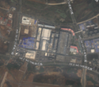
"Nursery plant"I was looking at YMTC's fab with Sentinel-2 satellite photos from this month. It looks like they topped off Fab 2.
View attachment 103593
Compare with how the Fab 1, 2 look like on Baidu maps with an image from several months ago.

And this is how it looks like on Google maps with only Fab 1 visible on even older photos.

Strategic fooyou agency strikes again
There is one Chinese company that will launch a series of X-ray metrology tools for 3DNand in the coming months. Probably already working hard to get their tools validated.we wouldn't know that and neither would he though, because he has no insight into YMTC's specific process.
From what I've heard, one problem is their dependence on KLA for 3D NAND dimensional metrology. 3D NAND poses specific problems due to high wafer bow from so many layered films causing strain in the wafer due to lattice mismatch and very high aspect ratio holes. This requires some unique capabilities such as small angle X-ray scattering.
There's plenty of scattering based optical techniques too, but those I don't know much about. Optical scatterometry is like black magic to me, so I don't qualify to talk about it.
Dimensional metrology is supposedly difficult to crack, it isn't just about lateral CD and point defect inspection (which can be taken care of by CD-SEM which China already has).
Hurun list of the 2030s might be filled with Semiconductors equipment bosses. What a decade.There is one Chinese company that will launch a series of X-ray metrology tools for 3DNand in the coming months. Probably already working hard to get their tools validated.
Having said that, even if China managed to have a complete and total supply chain inside the border. Do you think US & co just say "ggwp" and move on? Nah, I'm pretty sure deranged minds won't stay still. What else can they use to attack? Software? Global financial access?
Thank you for what you do, providing clear and fact-based analysis that cuts through the usual rhetoricI just published another article tonight on China semi that is for my subscribers only but will be online later in the week. Here is the title and bullets:
U.S. Sanctions Are A Catalyst For China’s New Semiconductor Fab Expansion
Dec. 18, 2022 9:05 PM ET, ,
Summary
- Current Chinese fab expansions through 2025 will add just 6% to the overall global semiconductor capacity with a $68 billion fab spend.
- Current 28nm fab expansions will only increase global capacity 4% despite sanctions.
- A recent Reuters article of a $142 billion Chinese fab spend and a subsequent suggestion of flooding of the low-end chip market is not based on reality.
- U.S. sanctions are minimally working, but only serve as a catalyst for China to promote its drive for self-sufficiency in chip making.
- Applied Materials is the greatest loser from sanctions as its YTD growth is 8.7% compared to its competitors' mean growth of 62.8%.
- Status
- Not open for further replies.

