Chinese semiconductor industry

Status
Not open for further replies.

tokenanalyst

Brigadier
Registered Member

Software and hardware collaboration: Guangli Micro accelerates the whole process solution for improving the yield of integrated circuit manufacturing​


Jiwei.com reported that Yield (Yield) is an important indicator of integrated circuit manufacturing, not only reflecting the technical value of the production line, but also a quantitative basis for continuous optimization of the process. Under the trend of shortage of production capacity, increasing the yield can directly increase the output value and reduce the manufacturing cost.

It is understood that the key to improving the yield rate lies in the effective monitoring and detection of the chip manufacturing process, and accurate and rapid analysis of massive monitoring data, identifying bottlenecks that limit the yield rate, preventing potential process risks in advance, and accelerating process upgrades and chip design optimization. .

Software and hardware synergy to create a yield ecology

In the wafer manufacturing process, it mainly includes process inspection methods such as physical inspection and electrical inspection. Wafer Acceptance Test (WAT for short) is the final electrical test for the quality control of the wafer when it leaves the factory. Through the test of the device and the test structure, relevant electrical parameters are obtained to characterize the process conditions and chip yield expectations.

It is understood that Guangliwei is one of the very few companies in China that can provide leading mass production electrical monitoring and yield improvement solutions, and has formed a "software and hardware synergy" yield ecology. The self-developed WAT testing machine has landed in the mass production lines and laboratories of several leading fabs, with EDA design tools, addressable (Addressable) and high-density (Dense Array) test chip technology, and DATAEXP data analysis platform Use to achieve design efficiency, effectiveness, and double the test speed. Through the standardized integration of the back-end production line database, a good data bridge and an effective closed-loop for yield feedback between upstream and downstream customers are established.


1272406889345.6946.png


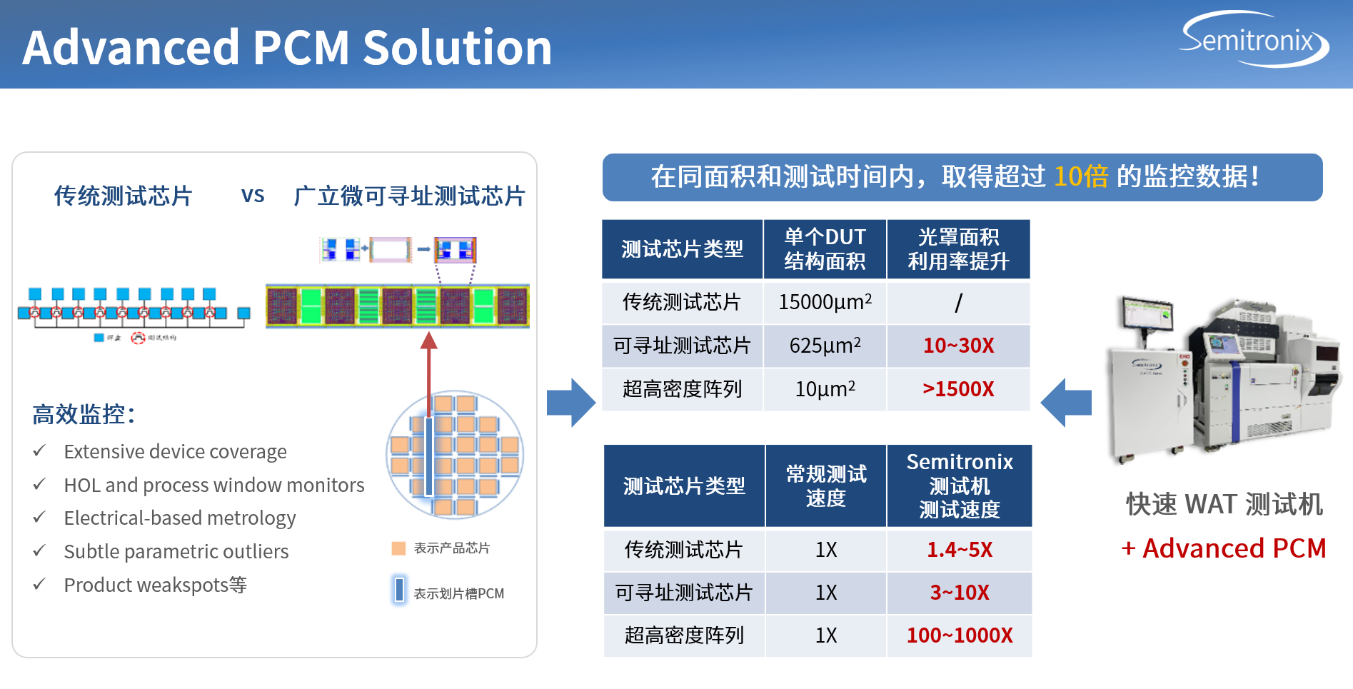
▲Software and hardware collaboration: quickly obtain more yield monitoring data

Guangliwei said, "Through the collaboration of software and hardware, our electrical monitoring solution can eliminate mines for the process development process, and the test efficiency can be increased by 10 to 1000 times. In addition, we also have a complete mass-produced electrical monitoring solution to ensure the stability of the domestic production line. It is understood that the company has recently developed an efficient mass production monitoring solution (Advanced PCM Solution) based on electrical testing, which can more accurately point to the root cause of yield failure during mass production.

Directly hit the pain points and shape all-round technical advantages

For electrical testing, test speed, cost, accuracy, comprehensiveness, and flexibility are all very important, but there are many difficulties in achieving efficient electrical testing, such as: accommodating more chips in a limited wafer area Test structure; improve design efficiency and design effectiveness through EDA software; improve test efficiency and control costs; realize data integration and analysis automation.

3574367822.919928.png


Guangliwei said that the company's Advanced PCM Solution covers a richer dimension of test content. In addition to the conventional yield monitoring structure, it has added related monitoring structures such as bottoming process windows, layout hotspots, device mismatches, and product sensitivity. Effectively conduct a comprehensive monitoring of the production line yield. High-density array technology can help chip design companies and fabs identify soft defects that affect yield at the ppm/ppb level (parts per million/parts per billion).

The traditional design scheme is limited by the number of pads, and the area utilization rate is low. However, Guangliwei adopts its own unique addressable technology, which can effectively improve the area utilization rate, increase the design unit density by 10-1500 times, and release more available area for dicing slots. The Advanced PCM Solution of Guangliwei achieves high-quality mass production through design and test collaboration; compared with traditional solutions, it reduces production costs, and in terms of yield monitoring and assurance, mass production line stability and predictability, etc., has obvious advantages.

Customized services to help fabs quickly achieve capacity expansion

In addition to technical advantages, Guangliwei also has a complete technical service team, which can tailor-made yield improvement programs based on specific needs of customers and provide diversified cooperation models. Guangliwei's partners already include: chip design companies (Fabless), wafer manufacturing plants (Fab), packaging plants (OSAT) and vertically integrated manufacturing companies (IDM).

Guangliwei said that the company has been formulating market strategies around the actual needs of customers and the technical pain points of the industry. Products and services that meet the needs of users.

Please, Log in or Register to view URLs content!
 

gadgetcool5

Senior Member
Registered Member
According to this, China is still struggling with domestic equipment maker due to dependency on foreign component

Please, Log in or Register to view URLs content!

Orders rise in short term, but domestic suppliers lag in supporting advanced semiconductor technology


It seems a gloom situation not only for YMTC and CXMT, I thought domestic equipment maker is already strong enough except the lithography..
Some of the issues mentioned in this article (if they are legitimate) could easily be remedied by government assistance, in increasing the salaries of employees in the equipment manufacturing sector; and also offering visas to American employees forced to become refugees if they want to continue to work in the sector.

This is clearly a more critical sector for China than chip design or manufacturing. China is being forced to sacrifice downstream for upstream. The key is to correctly gauge which downstream sectors can be sacrificed to help the upstream supply chain.
 
Last edited:

european_guy

Junior Member
Registered Member
Some of the issues mentioned in this article (if they are legitimate) could easily be remedied by government assistance, in increasing the salaries of employees in the equipment manufacturing sector; and also offering visas to American employees forced to become refugees if they want to continue to work in the sector.

This is clearly a more critical sector for China than chip design or manufacturing. China is being forced to sacrifice downstream for upstream. The key is to correctly gauge which downstream sectors can be sacrificed to help the upstream supply chain.

This is the only good piece of information in the whole article:

“The new sanctions are forcing companies like us to seek further co-operation with each other,” said an AMEC manager. “Executives from several companies, including ACMR, AMEC and others, are breaking walls and have had meetings on this.”

But the article is just the usual agenda-driven, ultra biased propaganda. Usually these articles come with 2 authors. One is local, and I guess is the one actually collecting info and writing the text, while the other is the "white supervisor" and ensures that the article follows the official narrative of the newspaper. His role is to remove too honest statements and instead add bias / copium / doomsaying etc.

After some practice you can even figure out which parts are from the original author and which are edited.
 
Last edited:

bzhong05

New Member
Registered Member
This is the only good piece of information in the whole article:

“The new sanctions are forcing companies like us to seek further co-operation with each other,” said an AMEC manager. “Executives from several companies, including ACMR, AMEC and others, are breaking walls and have had meetings on this.”

But the article is just the usual agenda-driven, ultra biased propaganda. Usually these articles come with 2 authors. One is local, and I guess is the one actually collecting info and writing the text, while the other is the "white supervisor" and ensures that the article follows the official narrative of the newspaper. His role is to remove too honest statements and instead add bias / copium / doomsaying etc.

After some practice you can even figure out which parts are from the original author and which are edited.
Seconded. In this regard, reading Chinese sources (EET-China, Ijiwei/Laoyaoba, Ofweek) is much more reliable and objective than Western MSM. Much of the MSM narrative on Chinese tech is usually 1) cherry-picking facts and worse still, many are not even factual but rather opinion-based (interview one analyst whose personal opinions can somehow represent a whole industry) 2) driven by a biased and doomsaying narrative (China did xxx, but at what cost?), and 3) overrepresenting a very small sample (aka equating one or two companies with an entire industry). Notice how there is very little trash talk about EVs or renewables? Because MSM can't make any of that stuff up when China dominates 80% of the value chain.

It also befuddles me how few of the "tech" journalists in MSM actually have a tech background or relevant expertise....
 

KYli

Brigadier
It would be better if China could have accessed to chips equipment from Japan and Dutch for a few months. But I think the West might have overplayed their cards and now there is only one way out for China that is to build its own chips industry from materials, equipment designs to manufacturing.
Please, Log in or Register to view URLs content!
“There’s no way China can build a leading-edge industry on their own. No chance,” said Sanford C. Bernstein analyst Stacy Rasgon.
 

Franklin

Captain
It would be better if China could have accessed to chips equipment from Japan and Dutch for a few months. But I think the West might have overplayed their cards and now there is only one way out for China that is to build its own chips industry from materials, equipment designs to manufacturing.
Please, Log in or Register to view URLs content!
“There’s no way China can build a leading-edge industry on their own. No chance,” said Sanford C. Bernstein analyst Stacy Rasgon.
There is no way of China to build a leading edge industry on its own in the short run. Yes that is true, but China doesn't have to build a leading edge industry in the short run only what its needs domestically that means for now 28 nm. That is more realistic.
 

european_guy

Junior Member
Registered Member
It would be better if China could have accessed to chips equipment from Japan and Dutch for a few months. But I think the West might have overplayed their cards and now there is only one way out for China that is to build its own chips industry from materials, equipment designs to manufacturing.
Please, Log in or Register to view URLs content!

If, as it seems, it will be a ban on equipment for sub 28nm, few months more do not change the big picture. To keep after-sales services and spare parts is more important. We will see what will be.

“There’s no way China can build a leading-edge industry on their own. No chance,” said Sanford C. Bernstein analyst Stacy Rasgon.

Yes, funny. But this one is a mister nobody, a random analyst, as you can get a dime a dozen.
 

tokenanalyst

Brigadier
Registered Member
It would be better if China could have accessed to chips equipment from Japan and Dutch for a few months. But I think the West might have overplayed their cards and now there is only one way out for China that is to build its own chips industry from materials, equipment designs to manufacturing.
Please, Log in or Register to view URLs content!
“There’s no way China can build a leading-edge industry on their own. No chance,” said Sanford C. Bernstein analyst Stacy Rasgon.
Let see about that. Surprises are ones of the beauty of life.
I my personal opinion, if China manage to make 28nm in volume on their own, it will mark the beginning of a big tectonic shift in the semiconductor industry.
 

tokenanalyst

Brigadier
Registered Member

This company can't stop giving.


ACM Shanghai enters PECVD market to support logic and memory chip manufacturing​


Launched Ultra Pmax TM PECVD equipment for the first time

Shengmei Semiconductor Equipment (Shanghai) Co., Ltd. (hereinafter referred to as "Shengmei Shanghai") (Science and Technology Innovation Board stock code: 688082), as a leading provider of wafer process solutions for semiconductor front-end and advanced wafer-level packaging applications The equipment supplier, today announced the launch of its proprietary Ultra Pmax TM plasma-enhanced chemical vapor deposition (PECVD) equipment, expanding an important new product category
. ACM Shanghai expects to deliver its first PECVD equipment to an IC customer in China within a few weeks.

1086406794993.2301.png


Wang Jian, CEO of Shengmei Shanghai, said:


"The launch of the Ultra Pmax TM PECVD tool marks our further expansion into new process domains in front-end semiconductor applications. Many of our customers are logic suppliers at 28nm and beyond. We anticipate capacity increases at mature process nodes , because the production capacity of mature process nodes in the Chinese market is obviously in short supply. This PECVD equipment enables Shengmei Shanghai to better serve global customers while meeting the needs of the global advanced logic and memory chip market. We predict that the launch of this Our new PECVD equipment and Ultra Lith, a pre-coating development equipment released last month, will double the size of our global serviceable market."

Features

Ultra Pmax TM PECVD equipment is equipped with chamber, gas distribution device and chuck design with independent intellectual property rights, which can provide better film uniformity, less film stress and less particle characteristics. The equipment adopts a single-chamber modular design and has two configurations: one can be configured with one to three-chamber modules, suitable for extremely thin film layers or fast process steps; the other can be configured with four- to five-chamber modules to optimize production capacity At the same time, it supports thick film deposition and longer process time. In both configurations, each chamber is equipped with multiple heated chucks to optimize process control and increase throughput.

Please, Log in or Register to view URLs content!
 
Status
Not open for further replies.
Top