the 'diameter' is the DeBroglie wavelength of the electrons, which is a quantum equivalent wavelength. The DeBroglie wavelength of electrons is FAR shorter than EUV. however, E-beam lithography is a direct write process, which means that the patterns are transferred sequentially to the resist. EUV lithography is projection lithography, so the entire pattern is transferred simultaneously, just like how a shadow of a complex shape is transferred to the wall at the same time (not strictly true for EUV, as it uses a reflection mask, but similar principle). The advantage is not noticable for simple patterns but when you have extremely complex patterns, it is very noticable (imagine drawing 500 million transistors sequentially, vs simultaneously).I read somewhere that electron beam lithography is more accurate than EUV lithography - because the diameter of electrons are smaller than the wavelength of EUV photons - but electron beam cannot be used for mass production commercially of IC chips because it is too slow a process... Is this true?

You are using an out of date browser. It may not display this or other websites correctly.
You should upgrade or use an alternative browser.
You should upgrade or use an alternative browser.
Chinese semiconductor industry
- Thread starter Hendrik_2000
- Start date
- Status
- Not open for further replies.
Bro from the video, I believed the chip they mention is Kirin 9100 14nm 3d chiplet with SMIC collaboration it means that Hisilicon did the packaging of unfinished SMIC 14nm chips.
broadsword
Brigadier
The automatic diamond growth furnace was successfully developed, and Jingsheng Electromechanical cracked the "ultimate semiconductor" material
Recently, Jingsheng Electromechanical technology research and development made another breakthrough and successfully developed a fully automatic diamond growth furnace.
01. The diamond crystal growth furnace was successfully developed, and a new member was added to the crystal growth equipment family
According to official sources, after more than half a year of process testing in Jingsheng Electromechanical Crystal Laboratory, the fully automatic MPCVD diamond growth equipment (model XJL200A) has successfully grown high-quality gem-level diamond crystals.
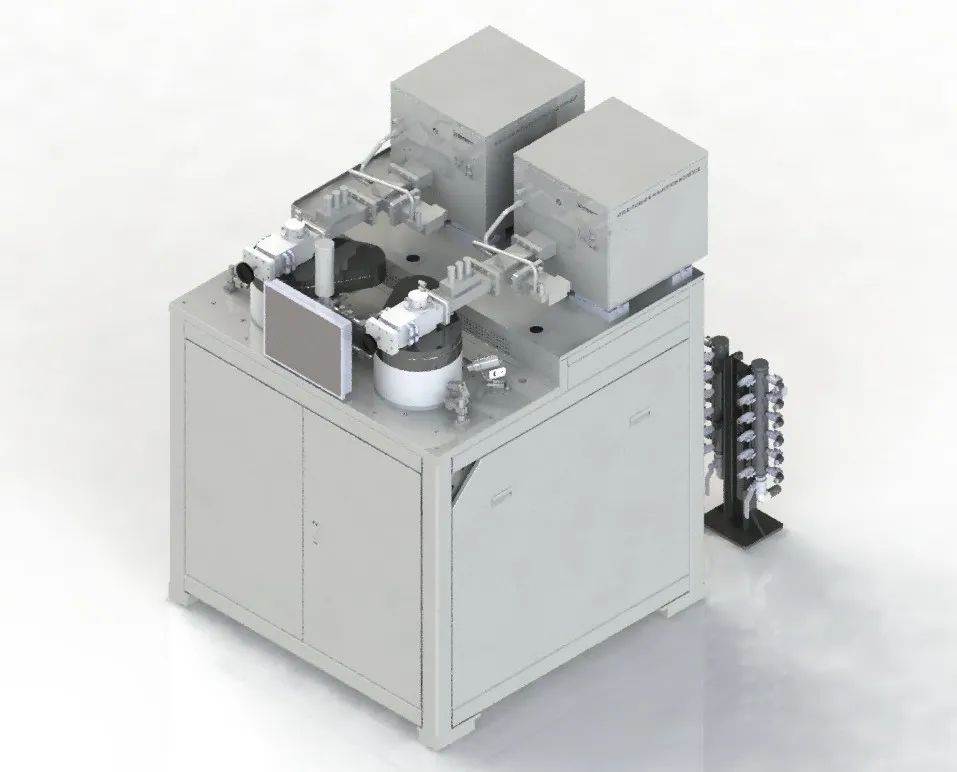
Image source: Jingsheng Electromechanical
According to reports, the XJL200A diamond growth furnace successfully solved the industry pain points of the traditional MPCVD diamond growth technology: the judgment of defects such as polycrystalline and growth cracks, and the control of key growth parameters such as crystal temperature and growth thickness all rely on manual judgment. , to overcome the current bottleneck of quality control and large-scale production in the process of artificially cultivated diamonds.
Is diamond crystal superior to silicon carbide and gallium oxide? Or are the applications different?
Wider bandgap than those two. Can operate under higher currents. Can withstand higher temperatures.Is diamond crystal superior to silicon carbide and gallium oxide? Or are the applications different?
The last one is a really big one. Clock speeds in silicon have stopped rising for more than a decade because of the heat removal problem.Wider bandgap than those two. Can operate under higher currents. Can withstand higher temperatures.
" We’ve always viewed YMTC as a company that one needed to monitor or understand, and they were potentially an emerging competitor,” Flores [Vice-chair of Kioxia] said, noting that the Chinese company had “leapfrogged” in technology after lagging behind bigger global rivals.
One of many, They make fun of SMIC, they had written off Huawei, CXMT and Fujian Jinhua, in 3 years time. We may see FT article depicting how Chinese tech company cheat and steal to overcome American restriction....lol" We’ve always viewed YMTC as a company that one needed to monitor or understand, and they were potentially an emerging competitor,” Flores [Vice-chair of Kioxia] said, noting that the Chinese company had “leapfrogged” in technology after lagging behind bigger global rivals.
- Status
- Not open for further replies.