Chinese semiconductor industry

Status
Not open for further replies.

european_guy

Junior Member
Registered Member
Please, Log in or Register to view URLs content!
At this year’s cseac, project 02’s project lead talked about the challenges facing China.

He explicitly called it "Sino-US technology war". I'm impressed. I also used that definition, but I'm just a random guy, not a very high level official doing a public conference.

US is playing hard ball here...but China accepted the challenge and is fighting back, without much fanfare, but possibly with even more determination and focus.
 

Weaasel

Senior Member
Registered Member
So this guy expended months unsuccessfully trying to convince Japan, Holland and other countries to join them, then they decided to go unilateral and rogue causing a lot of damage to companies all over the industry including to their own and their own allies companies, like South Korea that now their companies are begging to get an insignificant 1 year license.

Good luck, because non US companies are salivating for that market share and they are going to fight that, they have a very small window opportunity before Chinese companies take over the entirety of the Chinese market.

TEL has been accelerating their advertising in China about their tools as a one-stop solution for semiconductor manufacturing, just saying.
View attachment 100352
Chinese government should buy them on consignment for companies such as SMIC and YMTC, just in case of anything...
 

Weaasel

Senior Member
Registered Member
I read somewhere that electron beam lithography is more accurate than EUV lithography - because the diameter of electrons are smaller than the wavelength of EUV photons - but electron beam cannot be used for mass production commercially of IC chips because it is too slow a process... Is this true?
 

FairAndUnbiased

Brigadier
Registered Member
By this you mean one can build an advanced DUV fab possessing only Japanese equipment, substances (like photoresists), and other components, right?
yep. Japan has the capability to build a pure 45 nm fab at minimum with no new research, with no non-Japanese components at all. To get to 28 nm they may need some process research or consumables research like new resists. But otherwise they're OK.
 

tphuang

Lieutenant General
Staff member
Super Moderator
VIP Professional
Registered Member
New 12-inch fab in Shenzhen by Huarun Semi. 40nm. Car/Power related.

Please, Log in or Register to view URLs content!

I just wanted to post this other link regarding to cr micro on top of yours. Great example here of what's happening in the Chinese ic industry. They are about to start production on new 12 inch fab in Chongqing later this year with capacity of 30k wpm. Mostly mos and igbt power chips. They already produce power chips for cars, industrial product and new energy products. Total 7.55 billion rmb investment but large part of that paid off by govt in a jv. Significantly derisk the project for cr micro.

They also got another 8 inch fab under construction and now this new Shenzhen fab for 22 billion rmb. Which is a lot of money but Shenzhen govt and 3rd party investors pay a good portion of it and cr micro still controls 75% of jv. I wouldn't be surprised if smic jvs with local govt, they pay very little of the capex because they end up with normally 60% control of jv. Given the high margins of this business, the local govt can still get positive return of investment.

22 billion is a lot of money. Maybe they are looking for a 75k wpm fab. They must have received large orders.

I think this is the folly of American actions. Because they are no longer an industrial power, they completely ignore this segment. There is not question china will dominate this sector. They have all the tools to do so. And since most of world actually needs industrial and auto chips, they will end up relying on Chinese supply chain in 5 years or so. When it comes to the sanction, America is way too focused on the advanced nodes and ignore the harm on the mature markets

Once Chinese tool makers ramp up production, I don't see how lam and amat compete in this sector.

There has been no slow down in new projects or existing projects from what I can see in the advanced node. China is fully capable of supplying all the tools needed for 28 and more mature node now. The increased production of smee next year will fill the remaining gap.

Maybe the sanctions slowed down ymtc or smic, but even that is not so obvious.

He explicitly called it "Sino-US technology war". I'm impressed. I also used that definition, but I'm just a random guy, not a very high level official doing a public conference.

US is playing hard ball here...but China accepted the challenge and is fighting back, without much fanfare, but possibly with even more determination and focus.

I think you are right. The issue is that us govt right now is drunk on power so they don't think about the long term ramifications. We will see if they can force the Dutch govt to not allow asml supply china, because the speaker in this case very much discussed about the desire for globalization and finding trusted international partners. I don't think Japanese or Koreans will be persuaded to go in the other direction.

I don't think they can get Europeans to stop buying Chinese industrial chips. I don't think they can stop china from building fabs ok Europe that will bring jobs to Europe. So, what is the option? China's end goal is to produce a supply chain that centers around china that doesn't sanction other countries. In the end, if there are two main supply chain, the one that's cheaper, more customer friendly and less threatening will win. European govt tried their hardest to get the automakers to not work Chinese suppliers but VW is now all in with china because Chinese suppliers are the most convenient and best for value. Similarly, Korean and taiwanese semi industry that face American threat will bolt for the first alternative.
 

tokenanalyst

Brigadier
Registered Member
I read somewhere that electron beam lithography is more accurate than EUV lithography - because the diameter of electrons are smaller than the wavelength of EUV photons - but electron beam cannot be used for mass production commercially of IC chips because it is too slow a process... Is this true?
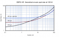
T (sec) = (Dose * Step Size^2)/ Current(nA)
Step size: A grid describing the feature. ie. 1nmX1nm, the large the grid the faster will print but uglier the features.

1667076351951.png
Dose:
1667074012452.png
Current: higher the current, large the beam size.

1667074715095.png

According to one paper the throughput could be as low as 24hr per cm2 i guess that with features size of less that 20nm.
A Pentium 4 with a die size of 1.28 cm2 with features size that range from 130nm the to 1200nm using a very sensitive photo-resist and reasonable grid size of 5nm, How much? like an entire day for just 1 exposure?
Just take into account that the 2011 SMEE 110nm ArF scanner had a throughput of 50 300mm wafers per hour, I guess.

this paper talk about how they increased speed times. is still low
Please, Log in or Register to view URLs content!

Once Chinese tool makers ramp up production, I don't see how lam and amat compete in this sector.
Well they can't compete even if they want to or are capable of, nanny goverment forbid them from doing so.
 
Last edited:

tphuang

Lieutenant General
Staff member
Super Moderator
VIP Professional
Registered Member
T (sec) = (Dose * Step Size^2)/ Current(nA)
Step size: A grid describing the feature. ie. 1nmX1nm, the large the grid the faster will print but uglier the features.

View attachment 100492
Dose:
View attachment 100489
Current: higher the current, large the beam size.

View attachment 100490

According to one paper the throughput could be as low as 24hr per cm2 i guess that with features size of less that 20nm.
A Pentium 4 with a die size of 1.28 cm2 with features size that range from 130nm the to 1200nm using a very sensitive photo-resist and reasonable grid size of 5nm, How much? like an entire day for just 1 exposure?
Just take into account that the 2011 SMEE 110nm ArF scanner had a throughput of 50 300mm wafers per hour, I guess.

this paper talk about how they increased speed times. is still low
Please, Log in or Register to view URLs content!
Well, it's been 10 years. Let's hope they are getting competitive in all these scanner products. The other option is just having to sell more of them to achieve the same throughput I guess.
Well they can't compete even if they want to or are capable of, nanny goverment forbid them from doing so.
Well, there are a whole lot of fabs for industrial and auto chips in Europe. If Chinese tool makers get competitive enough, they can sell that to European fabs. Just from what I can see, no slowdown in mature node expansion at all, so that volume of production has to lead to a lot of improvement in Chinese tool makers. If china is 50% of demand for mature node and American firms can't sell to this 50%, then Chinese tool makers will inevitably be the largest players in mature node and have the best product.
 

caudaceus

Senior Member
Registered Member
Bit OOT but anybody know why Germany's semiconductor (fabs,tools, materials, software , etc) aren't as bright as let's say their mechanical engineering prowess?
 
Status
Not open for further replies.
Top