Chinese semiconductor industry

Status
Not open for further replies.

gelgoog

Lieutenant General
Registered Member
Bit OOT but anybody know why Germany's semiconductor (fabs,tools, materials, software , etc) aren't as bright as let's say their mechanical engineering prowess?
Germany still has X-FAB and other fabrication facilities they inherited from Eastern Germany, Siemens used to be big in DRAM manufacturing even just a couple of decades ago, but they lost out to South Korean manufacturers after they made several missteps. They basically went into a technological dead end in terms of DRAM manufacturing technology and lost out. Bosch makes automotive grade electronics for vehicles like common rail systems for diesel engines, airbag control units, ABS, etc. I do not consider large fabrication facilities like GlobalFoundries in Dresden to be German companies though. It is just a foreign company with a US HQ which happens to have a fab in Germany.

As for the German semi fab tools sector being weaker I think it is just a reflection of them being weak in semi fabrication today in general. East Germany used to make its own fab tools, and Germany did use to have companies which made excimer lasers. Not any more. The global market for semi tools is really really small in number of units sold yearly and given the complexity required to make them there is a large enough barrier to entry. All the major semi tool vendors have good working relations with at least one of the major semi fabs. Once economies of scale start kicking in these companies are pretty much set. I think as Chinese fabs grow larger in scale they will increasingly start using Chinese tools. It is just how things are. The same thing happened in the CNC and industrial robot sector as China started to increase its own demand for such things.

China's semi fabrication capacity is already ahead of either Europe, the US, or Japan.

1667082983697.png
 
Last edited:

PiSigma

"the engineer"
Germany does do some software. For example there is SAP. OpenOffice/StarOffice also used to be written by Star Division in Germany. Cinema 4D which is the rendering software used in Cinebench is made by Maxon in Germany.

I think the reasons for Germany having a smaller software industry than other countries are they do not use English as a first language and their own market is much smaller than the one in other countries like the US. This means you will see several small sized companies but the really large software companies are much harder to come by. There is also a lot less capital in Europe that is willing to invest in new tech compared to the US or China.

As for the fab sector, Germany still has X-FAB and other fabrication facilities they inherited from Eastern Germany, Siemens used to be big in DRAM manufacturing even just a couple of decades ago, but they lost out to South Korean manufacturers after they made several missteps. They basically went into a technological dead end in terms of DRAM manufacturing technology and lost out.
Have you ever used SAP? Worst software on The face of the planet. I started using it 15 years ago and now it's on version 4 and it is still terrible. VW got their infotainment programing done in silicon Valley now, because the Germans couldn't do anything decent with the system.
 

caudaceus

Senior Member
Registered Member
Germany does do some software. For example there is SAP. OpenOffice/StarOffice also used to be written by Star Division in Germany. Cinema 4D which is the rendering software used in Cinebench is made by Maxon in Germany.

I think the reasons for Germany having a smaller software industry than other countries are they do not use English as a first language and their own market is much smaller than the one in other countries like the US. This means you will see several small sized companies but the really large software companies are much harder to come by. There is also a lot less capital in Europe that is willing to invest in new tech compared to the US or China.

As for the fab sector, Germany still has X-FAB and other fabrication facilities they inherited from Eastern Germany, Siemens used to be big in DRAM manufacturing even just a couple of decades ago, but they lost out to South Korean manufacturers after they made several missteps. They basically went into a technological dead end in terms of DRAM manufacturing technology and lost out. I do not consider large fabrication facilities like GlobalFoundries in Dresden to be German companies though. It is just a foreign company with a US HQ which happens to have a fab in Germany.
I'm sorry I wasn't clear, software here refers to EDA (even tho Siemens bought one) or other software for semiconductor industry.
 

tokenanalyst

Brigadier
Registered Member
Bit OOT but anybody know why Germany's semiconductor (fabs,tools, materials, software , etc) aren't as bright as let's say their mechanical engineering prowess?
-Zeiss
Please, Log in or Register to view URLs content!
-Trumpf
Please, Log in or Register to view URLs content!
-.pfeiffer-vacuum
Please, Log in or Register to view URLs content!
-Suss
Please, Log in or Register to view URLs content!
-aixtron
Please, Log in or Register to view URLs content!
Siltronic
Please, Log in or Register to view URLs content!
Heidelberg Instruments
Please, Log in or Register to view URLs content!

There will be no EUV machines without German technology, ASML won't be able to compete against Japanese companies without German technology. A lot of equipment makers from US, Europe, Singapore, Japan and China depend on parts from Germany. Pretty worrisome given the current energy crisis in Europe.
 

caudaceus

Senior Member
Registered Member
Have you ever used SAP? Worst software on The face of the planet. I started using it 15 years ago and now it's on version 4 and it is still terrible. VW got their infotainment programing done in silicon Valley now, because the Germans couldn't do anything decent with the system.
Some dark joke I heard is that SAP is German revenge for losing 2 world wars.
 

gelgoog

Lieutenant General
Registered Member
SAP is crap but then again so is Oracle and people do not stop buying that shit.

Germans were never that good at UI design so I find it hardly surprising that VW cannot make a proper car infotainment system. In my experience the French are better at UI design than the Germans are.
 

coldplasma

Just Hatched
Registered Member
I read somewhere that electron beam lithography is more accurate than EUV lithography - because the diameter of electrons are smaller than the wavelength of EUV photons - but electron beam cannot be used for mass production commercially of IC chips because it is too slow a process... Is this true?

I read something similar. Hence electron beam litography is used for the hard mask fabrication which is then used for DUV or EUV?
 

tokenanalyst

Brigadier
Registered Member

The automatic diamond growth furnace was successfully developed, and Jingsheng Electromechanical cracked the "ultimate semiconductor" material​


Recently, Jingsheng Electromechanical technology research and development made another breakthrough and successfully developed a fully automatic diamond growth furnace.

01. The diamond crystal growth furnace was successfully developed, and a new member was added to the crystal growth equipment family

According to official sources, after more than half a year of process testing in Jingsheng Electromechanical Crystal Laboratory, the fully automatic MPCVD diamond growth equipment (model XJL200A) has successfully grown high-quality gem-level diamond crystals.
20220308134459_%E5%BE%AE%E4%BF%A1%E5%9B%BE%E7%89%87_20220308134038.png

Image source: Jingsheng Electromechanical
According to reports, the XJL200A diamond growth furnace successfully solved the industry pain points of the traditional MPCVD diamond growth technology: the judgment of defects such as polycrystalline and growth cracks, and the control of key growth parameters such as crystal temperature and growth thickness all rely on manual judgment. , to overcome the current bottleneck of quality control and large-scale production in the process of artificially cultivated diamonds.

Please, Log in or Register to view URLs content!
 

tokenanalyst

Brigadier
Registered Member

Frontiers of Science and Technology | Great progress has been made in high-performance diamond quantum devices​


The Key Laboratory of Microscopic Magnetic Resonance, Chinese Academy of Sciences, University of Science and Technology of China has made important progress in the preparation of diamond quantum devices, and has developed a brand-new self-alignment-based photonics device preparation and processing technology, which can combine nitrogen-vacancy color centers at the atomic level The quantum sensor is processed to the optimal working position of the diamond device with nanometer precision, realizing a quantum sensor array with near-optimal optical detection performance. The research was published in Science Advances.


Diamond, commonly known as "diamond", has excellent physical and chemical properties such as high hardness, high stability, high light transmittance, high thermal conductivity and ultra-high forbidden band width. It is used in ultra-precision machining, optical materials and semiconductor electronic devices and other industries. field has a wide range of applications. In the past ten years, scientists have discovered that a kind of atomic-scale lattice defect in diamond that can emit light-nitrogen-vacancy color center (NV color center for short) has great quantum application prospects, making imperfect diamond with defects "perfect". Become more "perfect" in terms of practicality. NV color centers can not only precisely measure various physical quantities such as electromagnetic field and pressure with nanometer spatial resolution at room temperature, atmosphere and even extreme environments, but also can establish many-body quantum entanglement for the study of fundamental problems such as quantum information. , high-tech industries and other fields have significant application value.

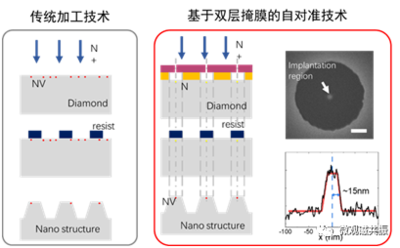
Figure 1: Schematic diagram of the preparation technology


The preparation of high-performance diamond quantum devices is the key technology for the practical application of diamond quantum information technology. Taking the diamond quantum sensor as an example, the principle is to use the NV color center in the device to convert the weak physical signal from the outside into an autofluorescence intensity signal for detection. Therefore, without sacrificing other physical properties, the photon count rate of the NV color center can be improved. It is a key indicator to improve sensor performance. In the past few years, active efforts have been made to develop diamond micro-nanophotonic structures for enhancing the fluorescence intensity of NV color centers, such as solid immersion lenses, cylindrical waveguides, circular bull's-eye gratings, parabolic reflectors, inverted nanocones, etc. . However, the current traditional preparation technology cannot precisely control the position of the NV color center in the micro-nano structure, resulting in low device preparation efficiency and difficult to achieve expected performance (Fig. 2(a)). The main reasons are the NV color center preparation process and diamond structure etching. Alignment challenges between processes (Figure 1 left). Usually this alignment accuracy needs to be better than 20 nanometers to achieve the theoretically optimal optical performance of the optical device.

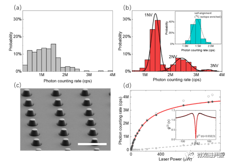
Figure 2: Demonstration of device fabrication. (a) Optical count rate distribution of devices fabricated by traditional process; (b) Optical count rate distribution of devices fabricated by self-alignment process; (c) Electron microscope photo of diamond nanopillar sensing array; (d) Fluorescence saturation curve test of a single NV color center.


For the above problems, the research team of this work has developed a photonics device processing technology based on a self-alignment strategy. Through the double-layer mask patterning process design, the nitrogen ion implantation process and diamond structure etching required for generating NV color centers are realized. The self-alignment of the etching process can achieve a precision of 15 nanometers (right in Figure 1). Using this technique, the research team achieved the fabrication of high-performance diamond nanopillar sensing arrays, which can be used for cutting-edge applications such as biosensing and nanoscale magnetic material imaging. Compared with conventional fabrication techniques, the devices show highly consistent and optimal photon count rates and device yields close to theoretical expectations. By further controlling the direction of the fluorescence emission dipole by the diamond crystal orientation, the team finally achieved a single NV color center saturation photon count rate of ~4.34Mcps, and the fluorescence intensity increased by about 20 times (Figure 2). The method has the characteristics of engineering, simplicity and high precision. It can not only prepare high-performance diamond quantum sensors in batches, but is of great significance to the practical application of diamond quantum technology, and can also be applied to other solid-state quantum systems such as silicon carbide and rare earth ions.


ChemChina focuses on the R&D and production of diamond, and has the ability to design MPCVD equipment. It is the first domestic company to master the core process of MPCVD to prepare high-quality diamond and achieve mass production, and it has created an original plasma-assisted polishing method for high-efficiency precision machining of diamond atomic-level surfaces. , Wafer-level diamond Ra<1nm, diamond heat sink thermal conductivity 1000-2000W/mk, more GaN on diamond, Diamond on GaN, diamond-based aluminum nitride and other products, used to solve high frequency, high pressure, high temperature, etc. In the future, we will continue to improve product quality through measures such as manufacturing intelligence and optimizing production processes, benchmarking against the international advanced management level, and continuously improve our products and services.
 
Status
Not open for further replies.
Top