You are using an out of date browser. It may not display this or other websites correctly.
You should upgrade or use an alternative browser.
You should upgrade or use an alternative browser.
Chinese semiconductor industry
- Thread starter Hendrik_2000
- Start date
- Status
- Not open for further replies.
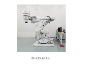
Ultra-precision robotic platform for lenses and optics polishing.
The Chinese Academy of Sciences' scientific research instrument and equipment development project "Large Aperture Optical Free-form Surface Ultra-Precision Robot Composite Processing Platform" undertaken by Shanghai Institute of Optics and Mechanics won the comprehensive acceptance excellent
Source: Release time: 2022-01-29 [Font: large, medium and small ] In December 2021, the Chinese Academy of Sciences' scientific research instrument and equipment development project "Large Aperture Free-form Surface Optical Component Robot Ultra-Precision Composite Processing Platform" undertaken by the Shanghai Institute of Optics and Fine Mechanics of the Chinese Academy of Sciences received excellent comprehensive acceptance. For the first time, the equipment has realized multi-functional, intelligent and ultra-precision grinding and polishing capabilities in a single robot carrier. The successful development of this equipment is of great significance for breaking the technical blockade of foreign optical processing technology and equipment.
Ultra-precision machining technology for large-diameter complex curved optical components is the core key technology in high-tech fields such as high-power lasers, space detection, and nanolithography. The existing box-type CNC polishing equipment has the defects of poor dynamic performance, insufficient flexibility and high cost. Robot polishing equipment is an effective means to solve the above problems, but it also faces the processing accuracy caused by low positioning accuracy, low rigidity and large vibration. Compared with foreign equipment of the same type, there is a big gap in our country.
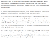
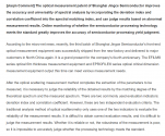
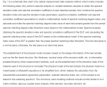
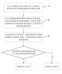
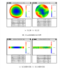
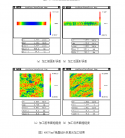
With the support of the institute's research and development projects, the team proposed the concept of a robot multi-functional processing platform, which innovatively integrated airbag polishing, jet polishing, flexible smoothing, and six-degree-of-freedom intelligent robot systems, realizing the effective integration of digital processing technology and intelligent robots. All kinds of complex surface grinding-polishing-finishing processes can be completed in a single equipment. Aiming at the bottleneck of high-precision machining of large-diameter optical components robot polishing full-band error, breaking through the mixed control of robot force, position, and attitude under different processes, adaptive path planning of complex surfaces, extremely narrow edge effects, sparse ripple control, and ultra-smooth surface generation, etc. The key technology has achieved a significant improvement in the polishing accuracy and efficiency of the multi-functional robot. The typical processing results are shown in Figure 1 and Figure 2.


antiterror13
Brigadier
nxt2100/2050i are special designed for China market, whose couldn’t get euv.
where did you get that ?
1. It is not listed on the website or any investor materialsI think they have a testing facility over there.
2. Why would you need an EUV for an OSAT facility? Makes no sense
I had been reading of such facility in Chinese internet for sometime. I know SMIC use to do stuff in Chengdu but I don't really know if they repurpose those facilities to R&D.1. It is not listed on the website or any investor materials
2. Why would you need an EUV for an OSAT facility? Makes no sense
When I say testing, I refer to a facility to test technologies, equipment and processes in way that doesn't disrupt their own normal operations, pretty much like the Shanghai ICRD or a kind of small R&D fab that can be scaled, this type of R&D facilities are usually no disclosed.
You know, I expected it would be the Japanese who would seize the opportunity to supply China while the Euros folded. Turns out ASML is stiff-arming America as hard as it can while Nikon lays like a useless pile. I guess that's why Japan is such a failure - even when it's presented with a golden opportunity on a silver platter, it has no initiative or gumption.nxt2100/2050i are special designed for China market, whose couldn’t get euv.
Japan has record of going with the wrong side of history, this time will be no exception.You know, I expected it would be the Japanese who would seize the opportunity to supply China while the Euros folded. Turns out ASML is stiff-arming America as hard as it can while Nikon lays like a useless pile. I guess that's why Japan is such a failure - even when it's presented with a golden opportunity on a silver platter, it has no initiative or gumption.
And Japan is known for technology Iteration with incremental improve on their product, like you said ASML act fast cause China will pay premium for those exclusive machine and its a win win, using their expertise from EUVL tech down to DUVL, those R&D will not go to waste as they have a ready and steady customer to sell.You know, I expected it would be the Japanese who would seize the opportunity to supply China while the Euros folded. Turns out ASML is stiff-arming America as hard as it can while Nikon lays like a useless pile. I guess that's why Japan is such a failure - even when it's presented with a golden opportunity on a silver platter, it has no initiative or gumption.
And by the way Nikon near equivalent to ASML NXT 2050i (MMO 1.5, 295 WPH) the NSR-S635E (MMO 2.1 , 275 WPH) is capable of producing 5nm chip and an improve variant the NSR-S636E is schedule to be release in late 2023 to compete with NXT 2100i. It's Nikon last hope as I expect that SMEE will be releasing its improve variant SSA900 22nm DUVL also next year. It will be an exciting year for all Chinese FAB makers as the three will battle it out, selling their advance ware instead of obsolete machine the US envisioned
Nikon Announces Development of the NSR-S636E ArF Immersion Scanner
October 18, 2021![[photo] [photo]](https://www.nikon.com/news/2021/img/10_nsr-s636e_01.jpg)
TOKYO - Nikon Corporation (Nikon) announced it is currently developing the next-generation NSR-S636E ArF immersion scanner, which will deliver superior overlay accuracy and ultra-high throughput to support manufacturing of the most critical semiconductor devices. Product sales are scheduled to begin in 2023.
As the digital transformation (DX) accelerates, there is an essential need to process and communicate tremendous volumes of data very quickly. High-performance semiconductors are imperative to satisfy these requirements, and semiconductor device technology is progressing with a simultaneous focus on circuit pattern miniaturization as well as 3-dimensional (3D) device structure development.
The NSR-S636E features an enhanced inline Alignment Station, or iAS, which is a wafer pre-measurement module integrated between the coater/developer unit and the lithography scanner. The S636E and iAS utilize sophisticated multi-point alignment measurement and high order correction functions that enable device makers to achieve the stringent overlay accuracy necessary for 3D device structures, while also maximizing immersion scanner productivity. The NSR-S636E is well-suited for cutting-edge semiconductor manufacturing including logic and memory devices, CMOS image sensor applications and more.
Nikon is committed to providing industry-leading lithography solutions like the NSR-S636E immersion scanner that enable customers to advance semiconductor manufacturing and help drive the digital transformation.
- Status
- Not open for further replies.

