Chinese semiconductor industry

Status
Not open for further replies.

tokenanalyst

Brigadier
Registered Member

Lenovo has started making cores! A shot is a 5nm chip​


Although Lenovo's 5nm chip is expected to be used in tablet computers, it is also a very difficult and risky move to use the most advanced technology for the first chip, which requires huge investment and R&D personnel support. It is unclear what the final result of this 5nm chip will be, but at least we see that Lenovo has really built a core, which is a huge improvement.
Recently, news came out that Lenovo's chip company Dingdao Zhixin's self-developed chip has been successfully taped out, and the 5nm process has been adopted. The next step will be related functional tests.
For a manufacturer with such influence in the field of PC and tablet, this self-developed chip is of great significance at present. According to another person familiar with the matter, "Lenovo's chip is specially designed for tablet PC applications."

Increase investment in the chip field

According to the information of Aiqicha, Dingdao Zhixin (Shanghai) Semiconductor Co., Ltd. was established in January 2022 and is 100% controlled by Lenovo. The company type is a wholly foreign-owned enterprise with a total registered capital of 300 million yuan. Its business scope For the design and sales of integrated circuits, as well as a number of businesses in the field of semiconductor technology.

Jia Zhaohui, the legal person and executive director of the company, was the senior vice president of Lenovo Group and the general manager of Lenovo Group's global consumer business and advanced innovation center. The general manager of the company, Shi Zhenggong, has worked in companies such as Leadcore, Huawei and OPPO. The company's SoC head Yuan Wei also has work experience in Leadcore. It is reported that Lenovo's chip team has more than 300 people.
The establishment of Dingdao Zhixin for chip self-research is only a small step for Lenovo. Lenovo Venture Capital has also invested in many local chip companies, such as Core Technology, Cambricon, Smartsens, Xinchi, Huaxing Semiconductor, Zhongke Wuqi, Ruisi Zhixin, Suzhou Huiwen, Onray Microelectronics, BYD Semiconductor, Yuguang Technology, etc.
In recent years, Lenovo has also participated in at least 8 investments related to integrated circuits, involving high-quality targets such as Jiehuat Microelectronics, Vodafone Semiconductor, Ruisizhixin, and Fullhan Microelectronics. In terms of coverage, Lenovo has invested in various applications in the integrated circuit industry, including at least AI chips, CMOS chips, IoT chips, 5G RF chips, IGBT chips, optical chips, single-photon sensor chips, semiconductor laser chips, smart audio and video. Processing SoC chips and other fields.

Please, Log in or Register to view URLs content!
 

FairAndUnbiased

Brigadier
Registered Member

Lenovo has started making cores! A shot is a 5nm chip​


Although Lenovo's 5nm chip is expected to be used in tablet computers, it is also a very difficult and risky move to use the most advanced technology for the first chip, which requires huge investment and R&D personnel support. It is unclear what the final result of this 5nm chip will be, but at least we see that Lenovo has really built a core, which is a huge improvement.
Recently, news came out that Lenovo's chip company Dingdao Zhixin's self-developed chip has been successfully taped out, and the 5nm process has been adopted. The next step will be related functional tests.
For a manufacturer with such influence in the field of PC and tablet, this self-developed chip is of great significance at present. According to another person familiar with the matter, "Lenovo's chip is specially designed for tablet PC applications."

Increase investment in the chip field

According to the information of Aiqicha, Dingdao Zhixin (Shanghai) Semiconductor Co., Ltd. was established in January 2022 and is 100% controlled by Lenovo. The company type is a wholly foreign-owned enterprise with a total registered capital of 300 million yuan. Its business scope For the design and sales of integrated circuits, as well as a number of businesses in the field of semiconductor technology.

Jia Zhaohui, the legal person and executive director of the company, was the senior vice president of Lenovo Group and the general manager of Lenovo Group's global consumer business and advanced innovation center. The general manager of the company, Shi Zhenggong, has worked in companies such as Leadcore, Huawei and OPPO. The company's SoC head Yuan Wei also has work experience in Leadcore. It is reported that Lenovo's chip team has more than 300 people.
The establishment of Dingdao Zhixin for chip self-research is only a small step for Lenovo. Lenovo Venture Capital has also invested in many local chip companies, such as Core Technology, Cambricon, Smartsens, Xinchi, Huaxing Semiconductor, Zhongke Wuqi, Ruisi Zhixin, Suzhou Huiwen, Onray Microelectronics, BYD Semiconductor, Yuguang Technology, etc.
In recent years, Lenovo has also participated in at least 8 investments related to integrated circuits, involving high-quality targets such as Jiehuat Microelectronics, Vodafone Semiconductor, Ruisizhixin, and Fullhan Microelectronics. In terms of coverage, Lenovo has invested in various applications in the integrated circuit industry, including at least AI chips, CMOS chips, IoT chips, 5G RF chips, IGBT chips, optical chips, single-photon sensor chips, semiconductor laser chips, smart audio and video. Processing SoC chips and other fields.

Please, Log in or Register to view URLs content!
Tablet is a good place to start with own chips: you don't need the best performance like desktop or best power efficiency like mobile, since many people use a tablet like a "light laptop" (I know I use my Lenovo 2 in 1 for that).

I'm glad Lenovo is finally going for it.

Is this going to be a x86 for Windows, ARM or RISC-V?
 

tphuang

Lieutenant General
Staff member
Super Moderator
VIP Professional
Registered Member
On ASML and SMIC,
Please, Log in or Register to view URLs content!

Back in March 2021, ASML completed a $1.2 billion order with SMIC for DUVs. Since these machines are close to $60 million each. One would surmise that SMIC purchased about 20 DUVs from Mar 2020 to Mar 2021. Since there was very little capacity expansion in the two 12-inch SMIC Beijing plants (maybe 10k wpm) during 2021, it's probably safe to assume that most of those DUVs were getting delivered for SN1 expansion.

As I mentioned here
My guess is that they are going eventually have something like. 20 DUVs should be plenty to cover this + a couple of extra DUVs needed in the Beijing fabs
10k wpm of 14 nm
10k wpm of N+1
15k wpm of N+2 or maybe even
20k wpm N+1 and 15k wpm of N+2 eventually
@latenlazy explained to me before that it normally takes some times to get new production lines worked out with new machines. It also likely took a while to receive other machines (due to sanctions and other reasons) and install them. As they work out their N+1/N+2 process, it's quite possible they did not have most of the lines fully work out until recently. Going by that theory, one would think the deliveries this year will be for the SN2 plant and the new Beijing/Shenzhen fabs.

Please, Log in or Register to view URLs content!
Article talked about the ASML fire incident from earlier this year. Apparently, SMIC signed a deal with ASML at the start of this year for delivery of a large number of DUVs. They are expected to be delivered throughout the year.

$60 million would've been around 50 million EUR at start of this year when contracts were signed. If we assume they are mostly just buying DUVi from ASML, then EUR 1.513 billion in first half would represent about 30 DUVs. If we assume that the fire from first half of this year was the reason for the lower deliveries in Q2 vs Q1, we could see full year delivery of 60 to 70 DUVs if the delivery rate is maintained for this year. Of which, HLMC, CXMT and YMTC may account for 10 to 20. So, I would guess a full year delivery of about 50 for SMIC, but we will have to see. It will likely supply for the initial 50k wpm production at Beijing fab + 40k wpm production at Shenzhen + whatever is needed for SN2. The first 2 would probably need about 10 to 15 DUVs if they are producing a mix of 28 nm, 40 nm, 55 nm and higher. The remaining 35 would allow them to fully devote SN2 for N+2 process and for installing in the new Shanghai LIngang fab. After which, there probably isn't need for more ASML DUVs at SMIC. My guess this year's order from SMIC will be their last major order with ASML. There is just too much sanction risk here. SMEE DUVs should be reliable by then for 28/22 nm production.


lol, even the guy at Tom's hardware picked up on this 14 nm news, along with the N+1/N+2 progress
Please, Log in or Register to view URLs content!

I had a thought just now. We know that SMIC has been mass producing 14 nm chips in their SN1 fab for a couple of years now (at least since 2020, what if that article about Shanghai company manufacturing 14 nm is actually talking about HLMC?

This is from 4 years ago
Please, Log in or Register to view URLs content!

In May of 2018, the first ASML DUV NXT 1980i was installed at the HLMC (Fab 6). It was said at the time that machines will be installed in Fab 6 over the next 5 months and that the production will reach 10k wpm by the end of that year. I also said there that they already mastered 55 to 28 nm by then (with most likely its Fab 5). The goal was to reach 40k a month by the end of this year. It has been more or less on track to do so, since it was likely at 30 wpm by end of last year based on this report page 12
Please, Log in or Register to view URLs content!
The explicit goal of this project was to be able to mass produce 28 to 14 nm chips. Given we are almost at the end of this expansion of fab 6 and it's been 4 years, it shouldn't be that difficult for them to be mass producing 14 nm chips by now.

Back in June of this year,
Please, Log in or Register to view URLs content!
reported that HLMC fab 6 reached some kind of new breakthrough. Although it says that HLMC had achieved 14 nm production techniques by 2020, it is quite possible they did not start mass producing it until first half of this year due to equipment delays and process maturation and such.
 

daifo

Major
Registered Member
Tablet is a good place to start with own chips: you don't need the best performance like desktop or best power efficiency like mobile, since many people use a tablet like a "light laptop" (I know I use my Lenovo 2 in 1 for that).

I'm glad Lenovo is finally going for it.

Is this going to be a x86 for Windows, ARM or RISC-V?

My guess would be ARM since Risc-v isn't ready for prime-time and intel doesn't offer x86 unless to avoid potential monopoly allegations.
 

AndrewS

Brigadier
Registered Member
@tphuang

You can see the variation in DUV prices for the different machines below

---

To set DUV against EUV is like comparing apples to oranges. On the EUV side, it’s simple. ASML currently has two EUV systems on offer that don’t differ all that much. One is a bit faster (170 wafers per hour) than the other (125 wafers per hour). The average purchase price of these systems last year was 145 million euros.

Within the DUV portfolio, the price differences are considerably larger. The most expensive DUV immersion systems use 193 nm light from an ArF laser and project their patterns through a water layer between lens and wafer. These cost around 60 million euros. The dry ArF systems fall into an entirely different price range, at around 20 million euros, while KrF machines cost 10 million euros.

I-line machines do not fall within the DUV category. They image patterns with the spectral i-line from a mercury lamp. For that type of system, ASML charges around 5 million euros.

---

Article below which also goes into what machines are required for each part of the chip stack, industry sales volumes, competition and where EUV is replacing DUV.

bits-chips.nl/artikel/we-underestimated-the-demand-for-duv/
 
Last edited:

ansy1968

Brigadier
Registered Member
@tphuang

You can see the variation in DUV prices for the different machines below

---

To set DUV against EUV is like comparing apples to oranges. On the EUV side, it’s simple. ASML currently has two EUV systems on offer that don’t differ all that much. One is a bit faster (170 wafers per hour) than the other (125 wafers per hour). The average purchase price of these systems last year was 145 million euros.

Within the DUV portfolio, the price differences are considerably larger. The most expensive DUV immersion systems use 193 nm light from an ArF laser and project their patterns through a water layer between lens and wafer. These cost around 60 million euros. The dry ArF systems fall into an entirely different price range, at around 20 million euros, while KrF machines cost 10 million euros.

I-line machines do not fall within the DUV category. They image patterns with the spectral i-line from a mercury lamp. For that type of system, ASML charges around 5 million euros.

---

Article below which also goes into what machines are required for each part of the chip stack, industry sales volumes, competition and where EUV is replacing DUV.

bits-chips.nl/artikel/we-underestimated-the-demand-for-duv/
Different MMO (Mixed Match Overlay)?

NXT 1980i = SMEE SSA 800 2.5NM

From @Oldschool

On September 3, 2021, the core Chengdu foundry, using the Shanghai microlithography machine SSA800/10W immersion lithography machine Parameters: Lens NA: 1.35 Single exposure resolution: 38-41nm Double workpiece stage: DWSi, yield Over-etching accuracy at 200 wafers per hour: better than 2.5nm Design index: able to meet the requirements of 28nm planar planner transistor logic circuit process under single exposure conditions

NXT 2000i 2.0NM

NXT 2050i 1.5NM

NXT 2100i 1.3NM

Please, Log in or Register to view URLs content!

Please, Log in or Register to view URLs content!


PDF

Sep 29, 2021 — NXT:2100i. 1.3 nm | 295wph. NXT:2050i. 1.5 nm | 295wph. NXT:2000i. 2.0 nm | 275wph. 1.35 NA, 38 nm. NEXT. DUV. (ArFi). Early Access. ASML.
 

hhuang41

New Member
Registered Member
Different MMO (Mixed Match Overlay)?

NXT 1980i = SMEE SSA 800 2.5NM

From @Oldschool

On September 3, 2021, the core Chengdu foundry, using the Shanghai microlithography machine SSA800/10W immersion lithography machine Parameters: Lens NA: 1.35 Single exposure resolution: 38-41nm Double workpiece stage: DWSi, yield Over-etching accuracy at 200 wafers per hour: better than 2.5nm Design index: able to meet the requirements of 28nm planar planner transistor logic circuit process under single exposure conditions

NXT 2000i 2.0NM

NXT 2050i 1.5NM

NXT 2100i 1.3NM

Please, Log in or Register to view URLs content!

Please, Log in or Register to view URLs content!


PDF

Sep 29, 2021 — NXT:2100i. 1.3 nm | 295wph. NXT:2050i. 1.5 nm | 295wph. NXT:2000i. 2.0 nm | 275wph. 1.35 NA, 38 nm. NEXT. DUV. (ArFi). Early Access. ASML.
SMIC does not have a foundry in Chengdu
Please, Log in or Register to view URLs content!
 

european_guy

Junior Member
Registered Member

What is in your opinion the future of EUV?​


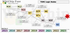
First of all a nice picture:

t0L4aARlFfrFrsUb.jpg

As you can see, when compared to 7nm, the performance speed up of a 3nm node at iso-power is less then 25% and we are 5 years and 2 full generations apart!

The real advantage of even smaller nodes is in logic density and power, not in performance.

But for which downstream application is this a critical advantage?

For smartphones probably it is. But for AI? For general computing and data centers?

When you don't have critical requirement on power consumption, you can use a 7nm and the impact will be very limited, but the cost advantage will be huge.

So my question is, what will be the future of EUV and sub 7nm nodes?

My take is that EUV is overrated. US is heavy investing in EUV sub 7nm nodes, but maybe they are betting on the wrong horse.

IMO China can do well just with DUVi for the foreseeable future with the only exceptions of smartphones chips. But these chips are not strategical. Chips for AI, autonomous driving, general computing and data-centers are. All these application have less constrains on power consumption.
 

56860

Senior Member
Registered Member

What is in your opinion the future of EUV?​


First of all a nice picture:

View attachment 97661

As you can see, when compared to 7nm, the performance speed up of a 3nm node at iso-power is less then 25% and we are 5 years and 2 full generations apart!

The real advantage of even smaller nodes is in logic density and power, not in performance.

But for which downstream application is this a critical advantage?

For smartphones probably it is. But for AI? For general computing and data centers?

When you don't have critical requirement on power consumption, you can use a 7nm and the impact will be very limited, but the cost advantage will be huge.

So my question is, what will be the future of EUV and sub 7nm nodes?

My take is that EUV is overrated. US is heavy investing in EUV sub 7nm nodes, but maybe they are betting on the wrong horse.

IMO China can do well just with DUVi for the foreseeable future with the only exceptions of smartphones chips. But these chips are not strategical. Chips for AI, autonomous driving, general computing and data-centers are. All these application have less constrains on power consumption.
Lithography machines and EUV is the only real roadblock to China's ambitions in semiconductors.
 
Status
Not open for further replies.
Top