Me too, I am just an enthusiast.please don't list me anywhere, I know very little. I'm the NEV guy.

You are using an out of date browser. It may not display this or other websites correctly.
You should upgrade or use an alternative browser.
You should upgrade or use an alternative browser.
Chinese semiconductor industry
- Thread starter Hendrik_2000
- Start date
- Status
- Not open for further replies.
bro your contribution is much appreciated, I learned a lot from you, 老师!Me too, I am just an enthusiast.
")
Phytium's D2000 is 2 years old now.
So SMIC has been producing 14nm since 2 years already...and only today it has been officially confirmed.
I was not able to find info on when the famous 7nm MinerVa Bitcoin Miner, analyzed by TechInsights, started production.
Anyhow it seems that SMIC is far more ahead of what they publicy announce. Maybe they are already in limited production also with the 7nm and nobody knows it until someone does not find another 7nm chip in the open market.
I also think is a bit suspect that all these advanced DUV immersion machines that landed in China in the last couple of years are dedicated to 28nm or above. From official statements it seems new SMIC fabs are all 14-28nm and above....I have some doubts on it....
The Bitcoin miner chip started production in July of 2021. It's probably among the first n+1 node that smic produced commercially. Back in 2020, smic said they would start n+1 trial production in April 2021. So all of the timeline here kind of work.
If you look here
In page 98, they think that SMIC developed the process for 14 nm back in 2019 and the process for N+1 (which is equivalent according to this as 8nm) back in 2020. Of course, trial production started later than that.
SMIC made Huawei's 710C Kirin SOC with its 14nm process back in 2020.
But Huawei has moved production of its Kirin 710 SoC, made for mid-range handsets, to SMIC from TSMC. The Kirin 710 was produced by TSMC using its 12MP process node and that will be replaced by the Kirin 710A made by SMIC using its 14nm FinFET process node. Chinese companies are believed to own 100% of the IP rights to the Kirin 710A.
In order to celebrate the mass production of SMIC's first 14nm FinFET chipset, all SMIC employees in Shanghai received an Honor Play 4T handset last week with the words "Powered by SMIC FinFET" printed on the back. Before the production of the Kirin 710A by SMIC, Huawei was using the Kirin 710F chipset. This had the same specs as the Kirin 710 with one change; using the "Flip Chip" manufacturing system, the component is able to carry more transistors inside without having to increase the size of the chip.
I am not a subject matter expert in semiconductor! I know little about architecture, business, software, overall process, etc. actually I rarely talk about chips or the chip business itself and if I do I'm just an enthusiast.When we reach 2000 pages, we should be entitled to Bachelor of Semiconductor studies lol.
Knowledge exposures from @FairAndUnbiased @tokenanalyst @tphuang et al are legendary
I only really know cleaning, etch, deposition. And more fundamental than business. more science paper than shareholder report so to speak.
Naura Solutions for Silicon Carbide Epitaxy.
Focusing on the third-generation semiconductors, NAURA is your trusted SiC product solution provider
The heart agrees, and everything is possible. Recently, NAURA was invited to participate in the "4th 3rd Generation Semiconductor Materials and Equipment Development Seminar". Dr. Liu Guangzheng, manager of compound process technology of CVD business unit, attended the meeting and gave a seminar with the theme of "Silicon Carbide Epitaxy Equipment Technology". Share the report.
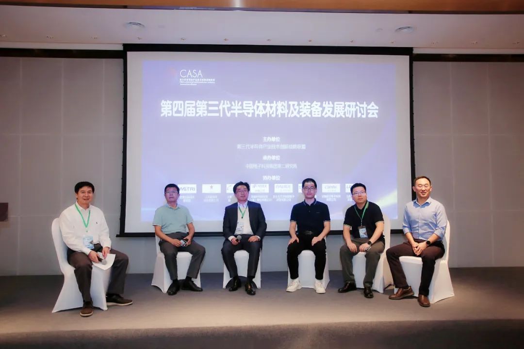
(The third from the right is Dr. Liu Guangzheng)
Driven by the development of terminal applications such as new energy vehicles, 5G communications, and photovoltaic energy storage, the third-generation semiconductor materials represented by silicon carbide (SiC) and gallium nitride (GaN) are gaining popularity. NAURA has an extensive layout in the field of SiC equipment, and various types of equipment have achieved large-scale application in domestic mainstream production lines, and can provide customers with comprehensive SiC product solutions. Among them, the cumulative number of orders for SiC crystal growth furnaces exceeds 2,000 units, and the cumulative number of orders for SiC epitaxy furnaces exceeds 100 units.
In terms of epitaxy equipment, NAURA has more than 10 years of technology accumulation in epitaxy equipment research and development, and has significant advantages in the design of temperature field, airflow field and platform control. It can customize development for a variety of semiconductor epitaxy equipment, covering the fields of silicon and compound semiconductors. .
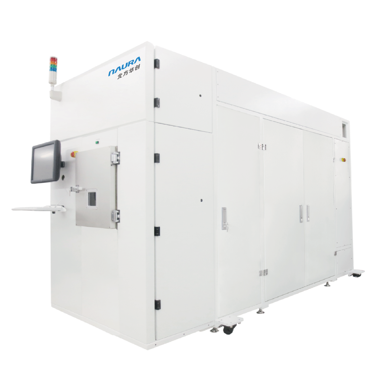
Among them, the MARS iCE115 silicon carbide epitaxy equipment adopts the horizontal hot wall technology route, as well as advanced temperature and pressure control algorithm, air intake structure and mixed flow structure, so that the thermal field and air flow field are uniform and stable during the entire epitaxy process, and process indicators such as uniform thickness The properties, doping concentration uniformity, defect density, etc. have all reached the advanced level in the industry. In addition, the machine design follows the IC concept, provides a complete security protection mechanism, and provides customers with a more convenient human-computer interface and various real-time data collection and monitoring functions.
At present, NAURA's 4/6-inch SiC epitaxy equipment has signed orders for more than 100 units, and batch machines have achieved stable mass production in major mainstream epitaxy plants.
As an advanced "solution service provider in the field of semiconductor basic products", NAURA will continue to deepen the field of semiconductor basic products, adhere to technology leadership, strengthen innovation drive, and bravely climb new heights.
Focusing on the third-generation semiconductors, NAURA is your trusted SiC product solution provider
The heart agrees, and everything is possible. Recently, NAURA was invited to participate in the "4th 3rd Generation Semiconductor Materials and Equipment Development Seminar". Dr. Liu Guangzheng, manager of compound process technology of CVD business unit, attended the meeting and gave a seminar with the theme of "Silicon Carbide Epitaxy Equipment Technology". Share the report.
(The third from the right is Dr. Liu Guangzheng)
Driven by the development of terminal applications such as new energy vehicles, 5G communications, and photovoltaic energy storage, the third-generation semiconductor materials represented by silicon carbide (SiC) and gallium nitride (GaN) are gaining popularity. NAURA has an extensive layout in the field of SiC equipment, and various types of equipment have achieved large-scale application in domestic mainstream production lines, and can provide customers with comprehensive SiC product solutions. Among them, the cumulative number of orders for SiC crystal growth furnaces exceeds 2,000 units, and the cumulative number of orders for SiC epitaxy furnaces exceeds 100 units.
In terms of epitaxy equipment, NAURA has more than 10 years of technology accumulation in epitaxy equipment research and development, and has significant advantages in the design of temperature field, airflow field and platform control. It can customize development for a variety of semiconductor epitaxy equipment, covering the fields of silicon and compound semiconductors. .
Among them, the MARS iCE115 silicon carbide epitaxy equipment adopts the horizontal hot wall technology route, as well as advanced temperature and pressure control algorithm, air intake structure and mixed flow structure, so that the thermal field and air flow field are uniform and stable during the entire epitaxy process, and process indicators such as uniform thickness The properties, doping concentration uniformity, defect density, etc. have all reached the advanced level in the industry. In addition, the machine design follows the IC concept, provides a complete security protection mechanism, and provides customers with a more convenient human-computer interface and various real-time data collection and monitoring functions.
At present, NAURA's 4/6-inch SiC epitaxy equipment has signed orders for more than 100 units, and batch machines have achieved stable mass production in major mainstream epitaxy plants.
As an advanced "solution service provider in the field of semiconductor basic products", NAURA will continue to deepen the field of semiconductor basic products, adhere to technology leadership, strengthen innovation drive, and bravely climb new heights.
Nevertheless you contribute a lot of valuable insight in terms of tracking the semiconductor industry development in China by providing us with the news and data, so I think your position in that list is wholly justifiedMe too, I am just an enthusiast.
Increasing cooperation between Chinese semiconductor equipment manufacturers.
Tuojing Technology(sypiotech): Domestic replacement not only needs to ensure quality and reliability, but also needs to keep up with customers to develop new technologies
Lv Guangquan, chairman of Tuojing Technology, pointed out that this general meeting of shareholders includes three proposals. The first proposal is to increase the quota for daily connected transactions in 2022, mainly including cooperation with China Micro Semiconductor Equipment Shanghai Co., Ltd. (hereinafter referred to as China Micro Company) (AMEC) , Shenyang Fuchuang Precision Equipment Co., Ltd. (hereinafter referred to as Fuchuang Precision) and Shenyang Scientific Instrument Co., Ltd. (RSIC semiconductor) of the Chinese Academy of Sciences (hereinafter referred to as Zhongke Instrument).
After the meeting, Lu Guangquan discussed the company's development and industry status with representatives of Aiji Micro's shareholders. He said that although domestic chip factories are currently undergoing large-scale expansion, the domestic production rate of equipment is still low. Under the wave of domestic substitution, local semiconductor equipment companies need to do a good job in two aspects, one is to improve the quality and reliability of their products, and at the same time to provide better services. The second is to develop new technologies and keep up with the pace of customers while participating in domestic substitution of mature products.
Regarding the proposal to increase the quota for daily related-party transactions in 2022, Zhao Xi, the secretary of the board of Tuojing Technology, pointed out that previously, the company reviewed and approved the "Proposal on Predicting the Company's Daily Related-party Transactions in 2022" at the 2021 Annual General Meeting of Shareholders. The annual amount of related party transactions is RMB 51.5 million. According to the needs of the company's business development and production and operation, the estimated amount of daily connected transactions in 2022 is increased by 69.5 million yuan. After the adjustment of the related party transaction quota, the daily related party transactions of the company in 2022 are expected to be no more than 121 million yuan.
Regarding the adjustment of the transaction quota of the three related parties, Zhongwei Company (AMEC) increased from the original 3.5 million yuan to 5.5 million yuan, Fuchuang Precision increased from the original 40 million yuan to 100 million yuan, and Zhongke Yi increased from 7.5 million yuan to 15 million yuan. Zhao Xi told Aijiwei that the company's specific related party transactions are mainly divided into two parts, one part is the purchase of raw materials or accepting labor services from related parties in the company's daily operations; the other part is to sell products to related parties.
Among the three related parties, Zhongwei Company directly holds 8.40% of the shares of Tuojing Technology Company, and Yin Zhiyao, chairman and general manager of Zhongwei Company, serves as a director of Tuojing Technology Company. In addition to direct investment, the two companies' day-to-day connected transactions also bring synergies to each other.
Previously, when Aijiwei communicated with Dr. Yin Zhiyao, chairman of the company at the general meeting of the company's shareholders, he pointed out that investing in Tuojing Technology Co., Ltd. is conducive to the three-dimensional development strategy of the company and the expansion of its business layout. Today, Lv Guangquan, chairman of Tuojing Technology, also pointed out that the company and China Micro Co., Ltd. cooperate in many aspects in film processing, and there are shared customers and shared suppliers, which can form a synergistic effect to a certain extent.
Talking about the company's development, Lu Guangquan told Aijiwei that the company's revenue in the first half of the year increased by 365% year-on-year, which was mainly due to two aspects: First, technological breakthroughs. In the first half of the year, the company's SACVD and ALD processes at 28nm and below New products have achieved results; second, a large number of shipments of traditional PECVD products have contributed to revenue growth.
In addition to business growth, Tuojing Technology also announced that it will invest 270 million yuan in Shanghai Lingang area to build a semiconductor equipment project, and is committed to quickly forming production and research and development capabilities, and to carry out research and development and industrialization of ALD. Lv Guangquan said that the Lingang subsidiary provides services to customers nearby, and provides production and technical support in concentrated areas. In addition, since new breakthroughs in the field also require continuous introduction of talents, it is more convenient for the subsidiary to register in Shanghai to attract talents.
New product release- Flux H Series - Variable Beam Laser System For Semiconductor Manufacturing Processes

Variable Beam Laser System Flux H Series

The application of laser technology continues to grow in breadth and depth, along with its rapid development. Higher requirements for laser energy, beam size and manufacturing technics keep increasing in various industries. For example, the requirements for more effective “line beam” and “area beam” have been implemented to replace the conventional “single point” lasers. Enhanced with the possibility of adjustable length and width, the line-shaped and area-shaped laser beams gained higher flexibility and are widely used in pan-semiconductor application solutions such as FPD & micro-LED, integrated circuit, lithium battery, glass and solar cell industries.

Features and Applications
01 Laser beam with 4kW power output/976nm wavelength
02 Continuously adjustable laser beam in width and length from 2-200mm
03 Beam uniformity > 95%
04 Temperature monitoring and closed-loop control
Powered by Focuslight’s core technologies in beam shaping and optical design, the Flux H series generates an adjustable laser beam with 4kW power output, 976nm wavelength from laser sources, and regulates the beam size and homogeneity through micro-optic modules. The beam is continuously adjustable in width and length from 2mm to 200mm, as the uniformity maintains as high as > 95%. Flux H has a flexible and versatile configuration with different beam size variation ranges and the corresponding working distances meeting specific application and processing requirements. It also integrates a high-speed pyrometer system that monitors the temperature of the processing area in real-time and carries out closed-loop temperature control.
The variable beam laser system Flux H series breaks the limitation of the fixed beam size in the conventional laser processing system. Through the adjustment of the embedded micro-optical modules, the beam length and width can be continuously adjusted in sections within the range of 2 - 200mm, as the uniformity maintains as high as > 95%. With the equipped coaxial pyrometer, the stability of processing can be guaranteed.

By flexibly selecting laser power and beam sizes, the variable beam laser system Flux H series works with a highly integrated processing head design and can be widely used in non-contact laser heating, laser assisted bonding, laser mass soldering, laser drying, material surface treatment and many more applications.
Variable Beam Laser System Flux H Series
The application of laser technology continues to grow in breadth and depth, along with its rapid development. Higher requirements for laser energy, beam size and manufacturing technics keep increasing in various industries. For example, the requirements for more effective “line beam” and “area beam” have been implemented to replace the conventional “single point” lasers. Enhanced with the possibility of adjustable length and width, the line-shaped and area-shaped laser beams gained higher flexibility and are widely used in pan-semiconductor application solutions such as FPD & micro-LED, integrated circuit, lithium battery, glass and solar cell industries.
Features and Applications
01 Laser beam with 4kW power output/976nm wavelength
02 Continuously adjustable laser beam in width and length from 2-200mm
03 Beam uniformity > 95%
04 Temperature monitoring and closed-loop control
Powered by Focuslight’s core technologies in beam shaping and optical design, the Flux H series generates an adjustable laser beam with 4kW power output, 976nm wavelength from laser sources, and regulates the beam size and homogeneity through micro-optic modules. The beam is continuously adjustable in width and length from 2mm to 200mm, as the uniformity maintains as high as > 95%. Flux H has a flexible and versatile configuration with different beam size variation ranges and the corresponding working distances meeting specific application and processing requirements. It also integrates a high-speed pyrometer system that monitors the temperature of the processing area in real-time and carries out closed-loop temperature control.
The variable beam laser system Flux H series breaks the limitation of the fixed beam size in the conventional laser processing system. Through the adjustment of the embedded micro-optical modules, the beam length and width can be continuously adjusted in sections within the range of 2 - 200mm, as the uniformity maintains as high as > 95%. With the equipped coaxial pyrometer, the stability of processing can be guaranteed.
| | | | |
| | | | |
By flexibly selecting laser power and beam sizes, the variable beam laser system Flux H series works with a highly integrated processing head design and can be widely used in non-contact laser heating, laser assisted bonding, laser mass soldering, laser drying, material surface treatment and many more applications.
I was just thinking a little more on SN1/SN2
For SN1, they spent 7.33 out of 9.06 billion USD on equipment -> 80.9%
For the first phase of Beijing plant, they estimated the investment to be 7.5 billion USd. If we assume about same non-equipment fixed cost, then they might be spending around 5.8 billion USD on equipment -> 77.3%. Seems reasonable.
So for 35k of 14 nm and under production, they are spend 7.33 billion. For 100k of 28 nm to 90 nm (probably mostly 28 nm to 55 nm), they are spending 5. 8 billion. So the average per wafer is about 3.6 times for SN1 vs the another 12-inch wafer plant that serves more advanced nodes.
Looking at the chart on Capex per wafer of different nodes (in section 2)
5 nm is a little under 4 times the cost of 28 nm
7 nm is about 2.9 times the cost of 28 nm
10 nm is about 2.1 times the cost of 28 nm
14 nm is about 1.6 times the cost of 28 nm
28 nm is about 1.3 times the cost of 45 nm
28 nm is about 1.57 times the cost of 65 nm
If we assume that the more advanced node fab is half 28 nm and the other half 45 to 90 nm, then it's likely the Capex for that factory is 1/1.3 = 0.77% of 28 nm. 3.6 x 0.77 is about 2.78 times. So SN1 capex is about 2.78 times that of 28 nm Capex per wafer.
it seems like SN1 is producing 14nm, N+1 (which is somewhere between 7 and 10nm) and N+2 (probably somewhere between 5 and 7 nm). Let's say N+1 is 2.6 times the cost of 28nm and N+2 is 3.5 times.
Then, I would say it's quite likely SN1 was allocated enough Capex budget to procure equipment for producing more N+2 and N+1 production and not that much 14 nm. If the estimates are true that they reached 15k wpm per end of 2021, then likely 10k of that is for 14nm and the remaining 5k is for N+1. Any additional capacity coming online is likely going into N+1 and N+2. That would also explain the additional ASML DUVi orders for the past 12 months. Based on my calculations, they are probably going to ramp up to have the following for SN1 based on Capex spending by middle of 2023.
10k wpm of 14 nm
10k wpm of N+1
15k wpm of N+2
My guess is that they have already bought all the equipment they need for SN1 by the end of Q1 if they are close to 30k wpm as @PopularScience said. Since work for SN2 seems to have started earlier this year, my guess is that any further ASML DUVs they purchased in Q2 onward will be for this fab. It's likely the ASML DUVi will be utilized in more advanced nodes. Beijing and Shenzhen plant could use a combination of older lithography machines and SMEE DUVi if they are just focused on 28 nm.
I'm assuming we will see a lot of new capacity for 28 nm to 90 nm segment coming online next year as the new Beijing fab start production and the existing 12-inch plants in Beijing reach their designed capacity. The plan is for this Beijing fab to reach 100k wpm by 2025. Looks like the Shanghai Lingang fab might start production in 2024 since it just started construction early this year.
Increasing cooperation between Chinese semiconductor equipment manufacturers.
Tuojing Technology(sypiotech): Domestic replacement not only needs to ensure quality and reliability, but also needs to keep up with customers to develop new technologies
After the meeting, Lu Guangquan discussed the company's development and industry status with representatives of Aiji Micro's shareholders. He said that although domestic chip factories are currently undergoing large-scale expansion, the domestic production rate of equipment is still low. Under the wave of domestic substitution, local semiconductor equipment companies need to do a good job in two aspects, one is to improve the quality and reliability of their products, and at the same time to provide better services. The second is to develop new technologies and keep up with the pace of customers while participating in domestic substitution of mature products.
A pretty good and accurate summary of what's going on in the broader Chinese market of semiconductor equipment manufacturing.
- Status
- Not open for further replies.