You are using an out of date browser. It may not display this or other websites correctly.
You should upgrade or use an alternative browser.
You should upgrade or use an alternative browser.
Chinese semiconductor industry
- Thread starter Hendrik_2000
- Start date
- Status
- Not open for further replies.
China Micro's MOCVD equipment has been verified on the customer's chip production line
"Science and Technology Innovation Board Daily" reported on August 23 that China Micro Semiconductor Equipment (Shanghai) Co., Ltd. stated that the company's MOCVD equipment for manufacturing GaN-on-silicon power devices has been verified on customer chip production lines. In addition, new MOCVD equipment for manufacturing Micro LED applications and epitaxy equipment for silicon carbide power device applications are also under development.
According to public information, China Micro Semiconductor Equipment (Shanghai) Co., Ltd. is a high-end micro-processing equipment company based in China and facing the world. By providing highly competitive high-end equipment and high-quality services to the world's leading semiconductor and LED chip manufacturers. China Microelectronics is based on high-end equipment fields spanning semiconductor chip front-end manufacturing, advanced packaging, light-emitting diode production, MEMS manufacturing and other micro-processes.
Does anyone know about China's gallium oxide production ability?
There was a recent article touting Japan's abilities recently, and about a ban to this technology.


Gallium oxide substrate wafers
● High-power and high-energy semiconductor devices: electromagnetic railguns, shipborne electromagnetic ejection systems, etc.
● Solar blind detection: fire monitoring, radar warning, near-Earth space communication devices, etc.
● High-power LED devices: high brightness, super large Power, scientific research inspection and detection equipment, etc.
UHV power transmission, urban rail and transportation power devices
4. China
In fact, my country has carried out research on gallium oxide for more than ten years, but it was not until the technological breakthrough of 46 institutes in recent years that it was "one step away" from industrialization. From the public information, we can understand the units and enterprises currently engaged in GaO material and device research, Mainly are 46 CLP, Xidian University, Shanghai Institute of Optics and Mechanics, Shanghai Institute of Microsystems, Fudan University, Nanjing University and other universities and research institutes. The companies that transform scientific and technological achievements include Beijing Gallium Technology, Hangzhou Fujia Gallium Industry . The domestic team has not seen any reports on GaO MOS.
(1) 46 Institutes of CLP
According to a report by Observer.com in February 2019, after years of exploration of gallium oxide crystal growth technology, the 46th Institute of China Electric Power Technology Co., Ltd. has effectively solved the problem of raw material decomposition and crystal growth during crystal growth by improving the thermal field structure, optimizing the growth atmosphere and crystal growth process. In 2016, the first high-quality 2-inch gallium oxide single crystal in China was successfully prepared by the guided mode method, and the first high-quality 4-inch gallium oxide single crystal in China was prepared by the end of 2018. crystal. The report pointed out that the width of the gallium oxide single crystal prepared by China Electronics 46 is close to 100mm, and the total length reaches 250mm, which can process 4-inch wafers, 3-inch wafers and 2-inch wafers. This is also the only domestic record holder that can reach this size so far.
(2) Xidian University/Institute of Microsystems
According to reports from Shanghai Institute of Microsystems and Information Technology, Chinese Academy of Sciences, in December 2019, Ou Xin's group, a researcher at the Shanghai Institute of Microsystems and Information Technology, Chinese Academy of Sciences, and Han Genquan, a professor of Hao Yue's group at Xidian University, joined hands to develop a gallium oxide New progress has been made in the field of power devices. Ou Xin's research group and Han Genquan's research group used the "universal ion knife" intelligent peeling and transfer technology to integrate wafer-level β-phase GaO single crystal thin film (400nm) with high thermal conductivity Si and 4H-SiC substrate wafer-level for the first time. and fabricated high-performance devices. The report pointed out that this work is of milestone significance in the field of ultra-wide bandgap materials and power devices. First, heterogeneous integration provides an optimal solution for the heat dissipation problem of GaO wafers, which is bound to promote the development of high-performance GaO device research; Promote the large-scale application of GaO in the field of high-power devices.
(3) Fudan University
In June 2020, Fang Zhilai's team from Fudan University made important progress in the research of p-type gallium oxide deep ultraviolet solar-blind detectors. According to the report, Fang Zhilai's team adopted the solid-solid phase transition in-situ doping technology, and achieved high doping concentration, high crystal quality and energy band engineering at the same time, thus partially solving the difficult problem of p-type doping of gallium oxide.
(4) Beijing Gallium Technology
According to the data, Beijing Gallium Technology Co., Ltd. was established at the end of 2017. It is the first domestic and the second international high-tech company specializing in the development and application industrialization of fourth-generation (ultra-wide bandgap) semiconductor gallium oxide materials. Teacher Tang Weihua from Beijing University of Posts and Telecommunications has been working on the industrialization platform of gallium oxide materials and devices to form scientific research achievements since 2011.
The company develops and produces high-quality single crystal and epitaxial substrates, high-sensitivity solar-blind UV detection devices, and high-frequency high-power devices based on the new ultra-wide bandgap semiconductor material gallium oxide. Tektronix diode model production, and has achieved 5000V withstand voltage MOSFET model production, developed gallium oxide-based solar-blind UV detector discrete devices and array imaging devices, providing a good solution for deep UV optoelectronic devices, which can support extremely weak flames And very weak arc real-time detection, etc., and has launched a systematic module. The company has applied for more than 40 patents, and has completed all the preparatory work for mass production requirements such as technology, personnel, software and hardware in the early stage of the industrial pilot test. The company has a plant area of 1,500 square meters, covering a complete industrial pilot production line, with R&D and small batch production capabilities, and has initially built a production and R&D platform for oxide single crystal substrates and gallium oxide hetero/homoepitaxial substrates. In the future, we will continue to improve the construction of six major platforms including crystal growth, crystal processing, epitaxial thin film performance testing, micro-nano processing, and joint research and development.
(5) Hangzhou Fujia Gallium Industry
According to the official website information, the company was established in December 2019 with a registered capital of 5 million. It was incubated by the Hangzhou Institute of Optics and Mechanics, a "hard technology" industrialization platform jointly built by the Shanghai Institute of Optics and Fine Mechanics of the Chinese Academy of Sciences and the Fuyang District Government of Hangzhou. technology-based enterprises.
Fujia Gallium Industry focuses on the research and development of wide-bandgap semiconductor materials. The core founders of the company have a deep background in the field of materials such as Ph.D. from the Chinese Academy of Sciences, and Ph.D. from Cambridge University. Reach 80%; the company's workshop area is more than 8,000 square meters, and it has a number of large-scale guided mode crystal growth furnaces, multi-atmosphere crystal annealing furnaces, high-precision polishing machines and other instruments and equipment, providing basic support for the company's development and continuous innovation. Power hardware ensure.
The original technology of Fujia gallium industry came from the technical research and development team of Shanghai Institute of Optics and Mechanics of the Chinese Academy of Sciences. Fujia Gallium Industry specializes in the design, simulation, growth and performance characterization of gallium oxide single crystal materials, which has formed relatively distinctive features and advantages. We focus on intellectual property protection and basic exploration and research work related to gallium oxide, and arrange patents for the growth of gallium oxide crystal materials and upstream and downstream applications on a global scale, and apply to enter the European Union, the United States, Japan, South Korea, Singapore and other countries. The team's basic research results on gallium oxide crystal materials and devices, and many scientific research papers have been published in top international academic journals, sharing the latest research results with global researchers, and jointly promoting the development of the world's fourth-generation semiconductor-related industries.
(6) Others
Shandong University used metal organic chemical vapor deposition (MOCVD) method to study the growth and optical properties of β-phase GaO thin films. Beijing University of Posts and Telecommunications, University of Electronic Science and Technology, and Sun Yat-Sen University have also independently carried out research on β-phase GaO thin films and solar-blind UV detectors, and have achieved some important research results, but there are basically no related reports on crystal materials.
Zhejiang University Hangzhou Science and Technology Innovation Center welcomes new achievements: the first batch of gallium oxide single crystal substrates!
Recently, the Hangzhou International Science and Technology Innovation Center of Zhejiang University (hereinafter referred to as the Science and Technology Center) successfully obtained the first batch of gallium oxide single crystal substrates . The center is capable of high-level research in the field of material processing.This batch of gallium oxide single crystal substrates was developed by the Semiconductor Materials Laboratory of the Advanced Semiconductor Research Institute of the Science and Technology Innovation Center. The conductivity type is semi-insulating, the size reaches 25.4 mm , the thickness is about 800 μm , the surface roughness is less than 0.5 nm , and the high-resolution X -ray The rocking curve test shows that the peak width at half maximum is 47.5 arcsec , the diffraction peaks are uniform and symmetrical, and the single crystal quality is good. The above key technical indicators have reached the advanced level in the field .
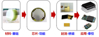
Research and development of Manufacturing equipment for Gallium Oxide Substrates.
Interesting story. looks its was not economically possible to mass produce this material without some change in the equipment used.
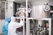
Recently, the 2022 "Technology Innovation China" annual conference with the theme of "Technology Self-reliance, Self-reliance and Entrepreneurship Drives Development" was held. At the meeting, the China Association for Science and Technology released the 2021 "Science and Technology China" series of lists. Among them, the "Leading Technology List" has selected 100 leading technologies with broad application scenarios and high economic and social benefits in six major fields, including biomedicine, resources and environment, electronic information, equipment manufacturing, advanced materials, and modern agriculture and forestry.
The "Heteroepitaxial Growth Technology and Core Equipment of Large-sized GaO Single Crystal Thin Films" independently developed by the research and development team led by Professor Wang Gang from the School of Electronics and Information Engineering (School of Microelectronics) of Sun Yat-sen University for more than ten years is the only project selected by universities in Guangdong Province. , is also the only selected project in Guangzhou. The technology developed by Wang Gang's team will form an industrial breakthrough in the field of emerging ultra-wide bandgap power semiconductor materials in China and even in the world, and will greatly promote the development and industrialization of gallium oxide-based power electronic devices in China.
The research results on the national list are behind the tenacity of Wang Gang's team for more than ten years. "Every time a door is opened, it takes constant exploration and repeated trial and error to find the next door." Wang Gang sighed to reporters.
When the reporter walked into the wide bandgap semiconductor material and device laboratory, generations of large-scale CVD equipment came into view. Wang Gang said that these are all CVD equipment purchased from abroad. "In 2006, we bought back this long-nitride machine from the UK. We had a hard time negotiating for a discount, but it also cost us nearly 10 million yuan." Wang Gang said.
In order to achieve a breakthrough from 0 to 1 in gallium oxide epitaxial materials and core equipment, Wang Gang led the team to develop MOCVD (metal organic chemical vapor deposition) equipment for heteroepitaxial growth of large-scale, high-quality gallium oxide semiconductor thin film materials. Large-scale heteroepitaxial growth process technology of gallium single crystal thin film materials.
"When we went to an academic exchange meeting, we heard Japanese experts share the prototype of gallium oxide power electronic devices. I thought we were equally capable of doing this, and we could go out of different technical paths, so we immediately started research after returning to China, and Heteroepitaxy was attempted with sapphire as the substrate." Wang Gang said that in the first two years, they were unable to grow thin film materials on the sapphire substrate. This feeling of suffocation and unpleasantness has always been unforgettable for Wang Gang. He also had doubts: Can this research direction really lead to success?
In anxiety and confusion, Wang Gang's team never gave up. Relying on the long-term research experience in nitride semiconductor components, they retrofitted an old MOCVD equipment for the production of second-generation semiconductor materials, and uniquely designed the reaction chamber of the semiconductor equipment. Over the past ten years, the team has continuously adjusted the process, parameters and design plans, and has accumulated experience in nearly 10,000 failures. In the end, they realized the independent development of MOCVD equipment for epitaxial growth of gallium oxide single crystal thin film materials, and they used the self-developed MOCVD equipment to grow crystals with high quality and uniform crystal orientation on large-scale heterogeneous substrates such as sapphire, silicon carbide and silicon. Good 4-8 inch ε phase gallium oxide single crystal film.
Multidisciplinary integration makes "black box" visualization
Wang Gang is filled with idealistic feelings. He told reporters that his goal in life is to develop better domestically produced equipment, and then grow better semiconductor materials.
Interesting story. looks its was not economically possible to mass produce this material without some change in the equipment used.

Wang Gang led the team to solve the key core problems in the industrialization of gallium oxide semiconductor materials.

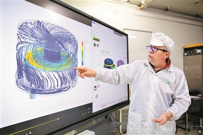
Wang Gang's team used digital modeling, digital twin and other technologies to visualize the reaction chamber.
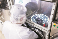
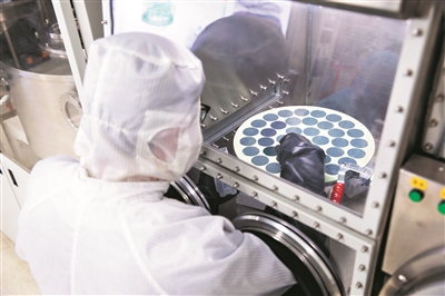
The research results on the national list are behind the tenacity of Wang Gang's team for more than ten years.


Wang Gang's team used digital modeling, digital twin and other technologies to visualize the reaction chamber.


The research results on the national list are behind the tenacity of Wang Gang's team for more than ten years.
Recently, the 2022 "Technology Innovation China" annual conference with the theme of "Technology Self-reliance, Self-reliance and Entrepreneurship Drives Development" was held. At the meeting, the China Association for Science and Technology released the 2021 "Science and Technology China" series of lists. Among them, the "Leading Technology List" has selected 100 leading technologies with broad application scenarios and high economic and social benefits in six major fields, including biomedicine, resources and environment, electronic information, equipment manufacturing, advanced materials, and modern agriculture and forestry.
The "Heteroepitaxial Growth Technology and Core Equipment of Large-sized GaO Single Crystal Thin Films" independently developed by the research and development team led by Professor Wang Gang from the School of Electronics and Information Engineering (School of Microelectronics) of Sun Yat-sen University for more than ten years is the only project selected by universities in Guangdong Province. , is also the only selected project in Guangzhou. The technology developed by Wang Gang's team will form an industrial breakthrough in the field of emerging ultra-wide bandgap power semiconductor materials in China and even in the world, and will greatly promote the development and industrialization of gallium oxide-based power electronic devices in China.
The research results on the national list are behind the tenacity of Wang Gang's team for more than ten years. "Every time a door is opened, it takes constant exploration and repeated trial and error to find the next door." Wang Gang sighed to reporters.
When the reporter walked into the wide bandgap semiconductor material and device laboratory, generations of large-scale CVD equipment came into view. Wang Gang said that these are all CVD equipment purchased from abroad. "In 2006, we bought back this long-nitride machine from the UK. We had a hard time negotiating for a discount, but it also cost us nearly 10 million yuan." Wang Gang said.
In order to achieve a breakthrough from 0 to 1 in gallium oxide epitaxial materials and core equipment, Wang Gang led the team to develop MOCVD (metal organic chemical vapor deposition) equipment for heteroepitaxial growth of large-scale, high-quality gallium oxide semiconductor thin film materials. Large-scale heteroepitaxial growth process technology of gallium single crystal thin film materials.
"When we went to an academic exchange meeting, we heard Japanese experts share the prototype of gallium oxide power electronic devices. I thought we were equally capable of doing this, and we could go out of different technical paths, so we immediately started research after returning to China, and Heteroepitaxy was attempted with sapphire as the substrate." Wang Gang said that in the first two years, they were unable to grow thin film materials on the sapphire substrate. This feeling of suffocation and unpleasantness has always been unforgettable for Wang Gang. He also had doubts: Can this research direction really lead to success?
In anxiety and confusion, Wang Gang's team never gave up. Relying on the long-term research experience in nitride semiconductor components, they retrofitted an old MOCVD equipment for the production of second-generation semiconductor materials, and uniquely designed the reaction chamber of the semiconductor equipment. Over the past ten years, the team has continuously adjusted the process, parameters and design plans, and has accumulated experience in nearly 10,000 failures. In the end, they realized the independent development of MOCVD equipment for epitaxial growth of gallium oxide single crystal thin film materials, and they used the self-developed MOCVD equipment to grow crystals with high quality and uniform crystal orientation on large-scale heterogeneous substrates such as sapphire, silicon carbide and silicon. Good 4-8 inch ε phase gallium oxide single crystal film.
Multidisciplinary integration makes "black box" visualization
Wang Gang is filled with idealistic feelings. He told reporters that his goal in life is to develop better domestically produced equipment, and then grow better semiconductor materials.
Sir with both Huawei and SMIC? what about Hua Hong?
Currently Hisilicon is the one using the 14nm 100% Domestic Line.Sir with both Huawei and SMIC? what about Hua Hong?
But SMIC and others will be adopting more of the Local equipment for their 14nm Production.
FABS in China now realise that in order to produce 14nm and 7nm Chips, it is a necessity to use Local Semiconductor Equipment and Local DUVL.
American and Japanese equipment are no longer reliable and a waste of Money.
SMIC has recently appointed Lu Hanming from the Chinese Academy of Engineering to its Board to help in the Localisation of Equipment.
There are rumours that Hisilicon has produced its own 28nm Immersion DUVL. It hired alot of talent from SMEE. Huawei wants to move faster and needs to make its own equipment.
The CETC 28nm Immersion DUVL is slated to be released later in the year.
Sir then Hisilicon should invest more on U-Precision, they're the one holding things up as they need capacity and investment to increase production.Currently Hisilicon is the one using the 14nm 100% Domestic Line.
But SMIC and others will be adopting more of the Local equipment for their 14nm Production.
FABS in China now realise that in order to produce 14nm and 7nm Chips, it is a necessity to use Local Semiconductor Equipment and Local DUVL.
American and Japanese equipment are no longer reliable and a waste of Money.
SMIC has recently appointed Lu Hanming from the Chinese Academy of Engineering to its Board to help in the Localisation of Equipment.
There are rumours that Hisilicon has produced its own 28nm Immersion DUVL. It hired alot of talent from SMEE. Huawei wants to move faster and needs to make its own equipment.
The CETC 28nm Immersion DUVL is slated to be released later in the year.
- Status
- Not open for further replies.
