Chinese semiconductor industry

Status
Not open for further replies.

tokenanalyst

Brigadier
Registered Member
Testing Chips with magnets?

Zhizhen Precision Instrument (Qingdao) Co., Ltd. is a national high-tech enterprise whose main business is the R&D and production of integrated circuit production line testing equipment and high-end scientific instruments. In the context of the rapid development of China's integrated circuit manufacturing industry and the urgent need for independent and controllable equipment in chip R&D and manufacturing, Zhizhen Precision Instrument has not yet achieved domestic success through independent innovation, industry-university-research cooperation, achievement transformation, and industry resource integration. Relevant high-end instruments and equipment with independent research and development capabilities have carried out engineering research.

Since its establishment in 2019, the company has gathered more than 50 talents of various types, and built an engineering team with a complete range of jobs in optics, electricity, precision machinery, measurement and control and automation, software and algorithms. , to introduce a number of expert-level talents. The company has successively established joint laboratories with Beihang University, Beihang University Qingdao Research Institute and Beihang University Hangzhou Research Institute to give full play to the advantages of industry-university-research integration to accelerate research and development. The company has subsidiaries in Beijing and Hangzhou. At present, the company has developed a series of domestic first sets of high-end equipment for the needs of the magnetic chip and integrated circuit manufacturing field, including China's first commercial magneto-optical Kerr microscope, industrial-grade wafer magneto-optical Kerr tester, etc. The products have been used in domestic top scientific research institutions and well-known integrated circuit manufacturing companies such as Tsinghua University and Chinese Academy of Sciences.

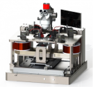
Wafer Level Magnetic Field Probe Series​


[Wafer level] Semi-automatic magnetic field probe station [1] Semi-automatic in-plane magnetic field probe station PS1DX-Auto8 3D renderings Project detailed parameters Magnetic field direction and maximum magnetic field strength In-plane magnetic field; ≥330 mT Whether the air gap is adjustable or not Size 12" Wafer (Backward Compatible with Fragment Test) Probe Type...
1661305451114.png

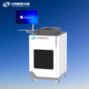
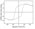
MOKE Hysteresis Loop Tester PL-MOKE​


Using the magneto-optical Kerr effect to measure the hysteresis loop of magnetic materials, the in-plane hysteresis loop and the vertical hysteresis loop can be measured synchronously.
1661305679028.png1661305691936.png

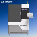
Wafer-MOKE​


The magneto-optical Kerr effect (MOKE) is used to rapidly and globally detect the magnetism of the wafer stack. Non-contact measurement avoids the damage to wafers caused by traditional magnetic characterization, and can be applied to sample inspection before and after patterning.
1661305900269.png
 

ansy1968

Brigadier
Registered Member
From my previous YT post about the 23 units of ASML DUVL delivered in the first quarter of this year had been confirm by this video below and to add a total of 78 units had been ship since last year nearing the 80 mark as posted by @Oldschool. IF the trend continue we may see a total of 180 units of ASML DUVL operating in China from the last 3 years alone.

Regarding TSMC, well they invested a lot in Taiwan for 3nm and 2nm tech despite Pelosi , the EU and the Japanese parliamentarian visit, some members here did call it right that their visits are more about Semiconductors. BUT TSMC opted to remain in Taiwan in a way showing their support for the motherland in a different way. Those technician and engineer will remain in Chinese hands instead of going to the Collective West. In case China mastered the EUVL tech, it will be a short boat ride away to harness those talents.

Please, Log in or Register to view URLs content!


Please, Log in or Register to view URLs content!


Please, Log in or Register to view URLs content!

2K views2 hours ago
 

MrCrazyBoyRavi

Junior Member
Registered Member
From my previous YT post about the 23 units of ASML DUVL delivered in the first quarter of this year had been confirm by this video below and to add a total of 78 units had been ship since last year nearing the 80 mark as posted by @Oldschool. IF the trend continue we may see a total of 180 units of ASML DUVL operating in China from the last 3 years alone.

Regarding TSMC, well they invested a lot in Taiwan for 3nm and 2nm tech despite Pelosi , the EU and the Japanese parliamentarian visit, some members here did call it right that their visits are more about Semiconductors. BUT TSMC opted to remain in Taiwan in a way showing their support for the motherland in a different way. Those technician and engineer will remain in Chinese hands instead of going to the Collective West. In case China mastered the EUVL tech, it will be a short boat ride away to harness those talents.

Please, Log in or Register to view URLs content!


Please, Log in or Register to view URLs content!


Please, Log in or Register to view URLs content!

2K views2 hours ago
Is this your youtube channel ? I had been watching this channel for sometime without knowing its from fellow SDF user. Good job
 

ansy1968

Brigadier
Registered Member
Is this your youtube channel ? I had been watching this channel for sometime without knowing its from fellow SDF user. Good job
Bro sorry you misunderstand , It's not mine I just post it, I apologized IF that inconvenience you. :(

And IF I do produce a YT Video I will use the sexy voice of @Loveleenkr plus her twitter video to attract viewership. ;)
 

WTAN

Junior Member
Registered Member
Sir then Hisilicon should invest more on U-Precision, they're the one holding things up as they need capacity and investment to increase production.
Yes more funding needs to be directed to these component manufacturers like U-Precision which are still small in size compared to their imternational peers. But things are changing and with the American Gift of sanctions, more funding will be directed to them.
 

PopularScience

Junior Member
Registered Member
Yes more funding needs to be directed to these component manufacturers like U-Precision which are still small in size compared to their imternational peers. But things are changing and with the American Gift of sanctions, more funding will be directed to them.
U-Precision received subsidy of 300 millions RMB each year from the government. This amount could employ several hundreds of engineers.
 

tokenanalyst

Brigadier
Registered Member
Yes more funding needs to be directed to these component manufacturers like U-Precision which are still small in size compared to their imternational peers.
I think U-Precision has not international peers. ASML does their own wafer stages and so is Nikon. So U-precision maybe the only independent company in the world making high end ultra precise wafer stages that i can think off.
 

FairAndUnbiased

Brigadier
Registered Member
Testing Chips with magnets?

Zhizhen Precision Instrument (Qingdao) Co., Ltd. is a national high-tech enterprise whose main business is the R&D and production of integrated circuit production line testing equipment and high-end scientific instruments. In the context of the rapid development of China's integrated circuit manufacturing industry and the urgent need for independent and controllable equipment in chip R&D and manufacturing, Zhizhen Precision Instrument has not yet achieved domestic success through independent innovation, industry-university-research cooperation, achievement transformation, and industry resource integration. Relevant high-end instruments and equipment with independent research and development capabilities have carried out engineering research.

Since its establishment in 2019, the company has gathered more than 50 talents of various types, and built an engineering team with a complete range of jobs in optics, electricity, precision machinery, measurement and control and automation, software and algorithms. , to introduce a number of expert-level talents. The company has successively established joint laboratories with Beihang University, Beihang University Qingdao Research Institute and Beihang University Hangzhou Research Institute to give full play to the advantages of industry-university-research integration to accelerate research and development. The company has subsidiaries in Beijing and Hangzhou. At present, the company has developed a series of domestic first sets of high-end equipment for the needs of the magnetic chip and integrated circuit manufacturing field, including China's first commercial magneto-optical Kerr microscope, industrial-grade wafer magneto-optical Kerr tester, etc. The products have been used in domestic top scientific research institutions and well-known integrated circuit manufacturing companies such as Tsinghua University and Chinese Academy of Sciences.

Wafer Level Magnetic Field Probe Series​


[Wafer level] Semi-automatic magnetic field probe station [1] Semi-automatic in-plane magnetic field probe station PS1DX-Auto8 3D renderings Project detailed parameters Magnetic field direction and maximum magnetic field strength In-plane magnetic field; ≥330 mT Whether the air gap is adjustable or not Size 12" Wafer (Backward Compatible with Fragment Test) Probe Type...

View attachment 96040

MOKE Hysteresis Loop Tester PL-MOKE​


Using the magneto-optical Kerr effect to measure the hysteresis loop of magnetic materials, the in-plane hysteresis loop and the vertical hysteresis loop can be measured synchronously.

View attachment 96042View attachment 96043

Wafer-MOKE​


The magneto-optical Kerr effect (MOKE) is used to rapidly and globally detect the magnetism of the wafer stack. Non-contact measurement avoids the damage to wafers caused by traditional magnetic characterization, and can be applied to sample inspection before and after patterning.

View attachment 96044
are they testing FRAM or something? Otherwise I'm not sure what ferromagnetics there are in a standard logic or memory chip.
 

FairAndUnbiased

Brigadier
Registered Member
Currently Hisilicon is the one using the 14nm 100% Domestic Line.
But SMIC and others will be adopting more of the Local equipment for their 14nm Production.
FABS in China now realise that in order to produce 14nm and 7nm Chips, it is a necessity to use Local Semiconductor Equipment and Local DUVL.
American and Japanese equipment are no longer reliable and a waste of Money.
SMIC has recently appointed Lu Hanming from the Chinese Academy of Engineering to its Board to help in the Localisation of Equipment.

There are rumours that Hisilicon has produced its own 28nm Immersion DUVL. It hired alot of talent from SMEE. Huawei wants to move faster and needs to make its own equipment.

The CETC 28nm Immersion DUVL is slated to be released later in the year.
I can believe this. I've seen many times where a company is better off making its own equipment which may not be commercially competitive if sold to exteral companies, but are still profitable if used internally. Usually you need to design around standard components as much as possible and have access to specialty machine shops for tricky components that can't be bought standard. For Hisilicon in particular it means their biggest challenge will be a light source supplier and water management system as these aren't exactly standard parts.

I don't know too much about lithography but for deposition instruments, you can assemble operational, R&D/pilot scale instruments from components relatively easily.
 

latenlazy

Brigadier
I can believe this. I've seen many times where a company is better off making its own equipment which may not be commercially competitive if sold to exteral companies, but are still profitable if used internally. Usually you need to design around standard components as much as possible and have access to specialty machine shops for tricky components that can't be bought standard. For Hisilicon in particular it means their biggest challenge will be a light source supplier and water management system as these aren't exactly standard parts.

I don't know too much about lithography but for deposition instruments, you can assemble operational, R&D/pilot scale instruments from components relatively easily.
If Huawei has made their own 28nm lithograph I would not be surprised if they more or less used the same design and central components as SMEE, and ended up with a machine that looks mostly identical. If they’re building for internal use only they can justify lower efficiency and reliability before adoption because they're not trying to turn the machine itself into a revenue positive business, and all the additional costs would be folded into the operations budget. It would essentially be an internal subsidy the company pays to itself to sustain the technological capability. This would be extremely expensive to the company if done at scale, but on the flip side they could move much quicker on the adoption learning curve and may be able to improve the quality of their instruments faster given that they could support utilization of their instrument at a loss well before their instruments reach quality and reliability levels comparable to the market.
 
Status
Not open for further replies.
Top