
You are using an out of date browser. It may not display this or other websites correctly.
You should upgrade or use an alternative browser.
You should upgrade or use an alternative browser.
Chinese semiconductor industry
- Thread starter Hendrik_2000
- Start date
- Status
- Not open for further replies.
In 2021 <> the number of R&D personnel will increase by 19.9% to 415.
This is a interesting piece of information. Does someone know about how many R&D people work at AMEC's competitor firms?
I'm surprised that you seemed surprised about the info on size of AMEC R&D team.This is a interesting piece of information. Does someone know about how many R&D people work at AMEC's competitor firms?
AMEC is very small compared to the big western WFE conglomerates. This shouldn't be a surprise. Still long way for domestic WFE companies to go to reach parity with the west.......or reach 70% make share.
Couldn't find the exact number of R&D people at AMAT/LAM, but maybe you can extrapolate from below stats (2021):
AMAT Revenue=$23B / R&D expense is $2.5B / 27,000 total employees
LAM Revenue=$16.5B / R&D expenses is $1.49B / 14,100 total employees
AMEC Revenue=$0.48B / R&D expenses is ~<$0.15 / <1,000 employees
Changdian Technology: Net profit of 860 million yuan in the first quarter of 2022, a year-on-year increase of 123%
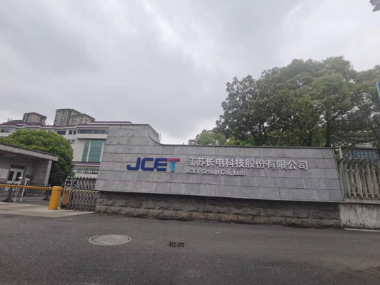
Jiwei.com news, on the evening of April 30, Changdian Technology announced that in the first quarter of 2022, the company's revenue was about 8.138 billion yuan, a year-on-year increase of 21.24%, and the net profit was about 860 million yuan, a year-on-year increase of 123.04%.
As for the reason for the increase in net profit, Changdian Technology said that the main reason is that the company continues to focus on high-growth and high-value-added products, actively optimizes customer and product structure, and improves profitability. At the same time, the company continued to take measures to reduce costs and increase efficiency, partially overcoming the pressure caused by rising material costs, power costs, and transportation costs, and maintaining continuous improvement in profitability.
According to the data, JCET is the world's leading provider of integrated circuit manufacturing and technical services, providing a full range of one-stop services for chip manufacturing, including integrated circuit system integration, design simulation, technology development, product certification, and in-wafer manufacturing. testing, wafer-level mid-pass packaging testing, system-in-package testing, chip finished product testing and can provide drop shipping services to semiconductor customers around the world.
@hvpc bro I discovered a YT video depicting the progress and History of China IC. I believed in China strategy of deployment (28nm and 14nm line) , present research (7nm line) and future research (5nm line ). The first one is heavy debated and we know that the SSA800 28nm DUVL is being deployed, with this machine and future improve iteration aside from producing 7nm with multi patterning, it can also do 5nm as the video disclose that Henan Research Institute has developed a fully automatic 12 inch wafer laser graving equipment which support 5nm DBG process. The domestic 7nm line will be finished by most optimistic timeline of mid 2023, as @WTAN once said IF your mastered 14nm finfet tech going down to 7nm is much easier cause you used the same equipment with a few tweaks. Now one by one as the video indicates they're trying their hands on 5nm line, with each breakthrough, I may surmised that a 5nm line will be available by late 2024 together with an Improved SSA900 22nm DUVL. I have confidences that China will reach its goal of Tech independence (of 7nm, 5nm and even an EUVL) within the next 3 years as multiple company however small will explore, research and innovate as survival and opportunity beckons.I'm surprised that you seemed surprised about the info on size of AMEC R&D team.
AMEC is very small compared to the big western WFE conglomerates. This shouldn't be a surprise. Still long way for domestic WFE companies to go to reach parity with the west.......or reach 70% make share.
Couldn't find the exact number of R&D people at AMAT/LAM, but maybe you can extrapolate from below stats (2021):
AMAT Revenue=$23B / R&D expense is $2.5B / 27,000 total employees
LAM Revenue=$16.5B / R&D expenses is $1.49B / 14,100 total employees
AMEC Revenue=$0.48B / R&D expenses is ~<$0.15 / <1,000 employees
208 views1 hour ag
Last edited:
To the opposite. OPPO and VIVO were founded by the same people, who are anything but pro-PLA.Soon, out of the blue, somebody would say that OPPO is related to PLA
Woah!!! France do a reverse and renew ties with Huawei with orders amounting to 234 billion yuan? IF true a big FXXK You to Uncle Sam.
5.7K views2 days ago
@ansy1968,@hvpc bro I discovered a YT video depicting the progress and History of China IC. I believed in China strategy of deployment (28nm and 14nm line) , present research (7nm line) and future research (5nm line ). The first one is heavy debated and we know that the SSA800 28nm DUVL is being deployed, with this machine and future improve iteration aside from producing 7nm with multi patterning, it can also do 5nm as the video disclose that Henan Research Institute has developed a fully automatic 12 inch wafer laser graving equipment which support 5nm DBG process. The domestic 7nm line will be finished by most optimistic timeline of mid 2023, as @WTAN once said IF your mastered 14nm finfet tech going down to 7nm is much easier cause you used the same equipment with a few tweaks. Now one by one as the video indicates they're trying their hands on 5nm line, with each breakthrough, I may surmised that a 5nm line will be available by late 2024 together with an Improved SSA900 22nm DUVL. I have confidences that China will reach its goal of Tech independence (of 7nm, 5nm and even an EUVL) within the next 3 years as multiple company however small will explore, research and innovate as survival and opportunity beckons.
208 views1 hour ag
I am aware of your views. I think you are lumping a lot of stuff together and making quite a bit of assumptions. Even though I am rooting for China's semiconductor progress, I do not share your assessment of our current situation. I'm actually not happy about the progress we are making as I think the gap to target is not closing fast enough. I'm a bit frustrated, actually.
I think it's futile to debate and try to get us to take on the other's assessment this is why I don't make posts on my personal feeling, assessments, or speculations, etc. I also don't try to educate or "teach" in case people interpret it as me talking down to people. I now try to as much as possible only posts and share actual information or respond to questions. I often draft long responses only to delete them before sending because I'm trying not to create controversy as much as possible.
So let's agree to disagree, if that's alright with you.

Last edited:
Intel has spent a long time trying to shrink their transistors more with immersion DUV litho and so far it has been a failure.
One reason why TSMC is ahead of Intel right now is they went big on EUV before them while Intel gave up on EUV despite being an early proponent like a decade ago. Now Intel plans to jump straight into high NA EUV from what I understand.
One reason why TSMC is ahead of Intel right now is they went big on EUV before them while Intel gave up on EUV despite being an early proponent like a decade ago. Now Intel plans to jump straight into high NA EUV from what I understand.
Actually, the reason for Intel's failure with 10 nm is their insistence on cobalt interconnects and contact over active gate (COAG). These are still not attempted by the TSMC. Intel tried to leapfrog everyone and paid for that.Intel has spent a long time trying to shrink their transistors more with immersion DUV litho and so far it has been a failure.
One reason why TSMC is ahead of Intel right now is they went big on EUV before them while Intel gave up EUV despite being an early proponent like a decade ago. Now Intel plans to jump straight into high NA EUV from what I understand.
- Status
- Not open for further replies.