Chinese semiconductor industry

Status
Not open for further replies.

FairAndUnbiased

Brigadier
Registered Member
third party service companies are usually only brought in after the tool is end-of-life. At that stage of the product life, the original WFE supplier will usually provide manuals or training for a smooth hand-off. But in the scenario we are talking about, no way the WFE supplier will train anyone to service systems in China while the actual product is still "active" in the product life cycle. It would become quite a dilemma for the fab to decide if they want to risk a third party company coming in and damaged a $80M or more system further. I don't think third party would willing to take a risk either.

Laser is actually paid for by use. So when it's near end of life, Cymer or Gigaphoton will come to replace it. Optics do degrade and would impact the efficiency of the system but can be in use for a long time.
I know that at the very least, I've seen refurbished components being cleaned and tested to ASML GSA specifications which is based around EUV. I don't believe that any EUV equipment is EOL. Not my department but I did do some custom instrument buildouts for them and know most of their processes.

Also, for most vacuum chamber tools at the very least, you have some universal principles in cleaning specification, chamber coatings, and how to refurbish major components. You also have interchangeable parts on many wear components, even multiple suppliers on one part.

The other thing is, for many major 3rd party service and parts OEM companies, you can contract for a special project. Instead of technicians coming out for routine repairs, an engineering or even R&D team can figure out for you how to keep your system running and what parts to provide. You'd be surprised what you can get on the open market. 3rd party suppliers aren't small fly by night operations either, many are billion+ companies that also act to supply the major integrators with components.
 

hvpc

Junior Member
Registered Member
I know that at the very least, I've seen refurbished components being cleaned and tested to ASML GSA specifications which is based around EUV. I don't believe that any EUV equipment is EOL. Not my department but I did do some custom instrument buildouts for them and know most of their processes.

Also, for most vacuum chamber tools at the very least, you have some universal principles in cleaning specification, chamber coatings, and how to refurbish major components. You also have interchangeable parts on many wear components, even multiple suppliers on one part.

The other thing is, for many major 3rd party service and parts OEM companies, you can contract for a special project. Instead of technicians coming out for routine repairs, an engineering or even R&D team can figure out for you how to keep your system running and what parts to provide. You'd be surprised what you can get on the open market. 3rd party suppliers aren't small fly by night operations either, many are billion+ companies that also act to supply the major integrators with components.
Intersting. Thanks for sharing.

When I was in the fab we have service contract with ASML for all our scanners that are not EOL. I thought all fabs do it the same way.

Sounds like you are part of ASML's supply chain. Are you allowed to sell your service to any fab or are you bound by NDA with ASML to only refurbish parts for them? If no such limit then you guys could make big buck offering your service to fabs because ASML service contracts are not cheap.
 

FairAndUnbiased

Brigadier
Registered Member
Intersting. Thanks for sharing.

When I was in the fab we have service contract with ASML for all our scanners that are not EOL. I thought all fabs do it the same way.

Sounds like you are part of ASML's supply chain. Are you allowed to sell your service to any fab or are you bound by NDA with ASML to only refurbish parts for them? If no such limit then you guys could make big buck offering your service to fabs because ASML service contracts are not cheap.
Typically in my experience, 3rd party companies are not allowed to service fabs directly for lithography systems because we all have different expertise. For instance a chemical systems or high purity parts supplier have no capability in optics. There are likely other service companies out there with this capability, but not in say, high purity materials.

So everything for ASML goes through ASML or an ASML primary contractor. We are admittedly a minor contributor to ASML as they do not use our primary expertise very well. Much more work is done with deposition/etch equipment and chemicals. However, if a customer knows what parts they need or has a specific request for problem solving that falls within the correct domain, this is possible to do long term service. This was done many times for analog and mixed signal fabs.

We have not worked with leading edge logic fabs directly though. I imagine things there are much more tightly regulated. Many analog and mixed signal fabs, even majors, heavily depend on a mix of new and old equipment that they put together themselves.
 
Last edited:

Appix

Senior Member
Registered Member
I agree but still Chinese tech companies need a risk rate system to catalog their supply chain from low risk to high risk, personally for now I would put everything made in the U.S. in the top of the list with the highest risk of being interrupted and in need of replacement as soon as possible. There is a high possibility that China hawks will take control of the export control narrative in the White House in 2024 if Trump wins the election.
COVID may be a temporary problem but braindead Americans Politicians willing to hurt their own companies in the hope of hurting China are a permanent one.

Please, Log in or Register to view URLs content!
Here is a non-paywall version of the article.

Please, Log in or Register to view URLs content!
 

Overbom

Brigadier
Registered Member
Please, Log in or Register to view URLs content!
I got to give it to them, that's some hardcore hopium:
Defining what equipment can still be exported to China may prove too difficult. But if it works, Chinese chipmakers would need decades to catch up with the West. And America would have met the goals of suppressing Chinese semiconductor development while causing minimal harm to its own industry.

At this point the Jai Hinders are more rational than whoever writes this kind of stuff.
 

FairAndUnbiased

Brigadier
Registered Member
I got to give it to them, that's some hardcore hopium:


At this point the Jai Hinders are more rational than whoever writes this kind of stuff.

It does take a while for fabs to integrate new process equipment. Not just equipment installs but you need to run test wafers to assess, for instance, CD and uniformity for the process.

But when it's integrate new process equipment or go out of business, things tend to take on new urgency.

Btw, YMTC already purged it's supply chain of US components and equipment as much as possible and is continuing to do more.

Please, Log in or Register to view URLs content!
 

caudaceus

Senior Member
Registered Member
It does take a while for fabs to integrate new process equipment. Not just equipment installs but you need to run test wafers to assess, for instance, CD and uniformity for the process.

But when it's integrate new process equipment or go out of business, things tend to take on new urgency.

Btw, YMTC already purged it's supply chain of US components and equipment as much as possible and is continuing to do more.

Please, Log in or Register to view URLs content!
As long as it's not decades then that's good enough.
I really hope that IC in the future will be so commoditized just like steel today, then even low to mid-income countries can build their own fabs.
 

FairAndUnbiased

Brigadier
Registered Member
As long as it's not decades then that's good enough.
I really hope that IC in the future will be so commoditized just like steel today, then even low to mid-income countries can build their own fabs.
IC is actually surprisingly not that bad - as long as you don't chase the leading edge. if you accept KrF 130 nm process as your limit or stick to 200 mm, you can do a ton of stuff like microcontrollers, power, RF, analog, optoelectronics, etc. You can basically build industrial robots, car chips, LEDs, radios, TVs, etc. with that. However, it's not cost that is the limitation, it's the educational infrastructure. Many poorer countries outright don't have enough people with the understanding of materials science, physics, chemistry, engineering, etc. to do semiconductors. The only countries where education isn't an issue, only cost, is Eastern Europe. Russia already has fabs like this using older tech pushed to its limits. Ukraine apparently used to have a fab, clearly that's no longer the case.

just as an example of what old processes can do with the knowledge of design, processes and materials we have today, YMTC's memory I/O circuit for its leading edge 128 layer NAND flash is done on 180 nm process. It is possible for YMTC to use different process sizes on the memory array portion and the I/O readout portion because their IC packaging scheme separates the 2 wafers (I/O chip is separate from the memory itself) then bonds them together.

Please, Log in or Register to view URLs content!

So how good is it? According to the reviewer, 180 nm process is good enough for 3 Gb/s readout which is apparently 2x faster than conventional readouts with CMOS under array. But the CMOS under array type chips (where you fabricate the I/O and logic as the bottom layer on a wafer then build the array on top of them) are likely built with 16-20nm process throughout which is far more expensive. So despite using a more advanced process for the logic portion, standard chips perform worse than a cheaper process with optimized architecture.
 

hvpc

Junior Member
Registered Member
IC is actually surprisingly not that bad - as long as you don't chase the leading edge. if you accept KrF 130 nm process as your limit or stick to 200 mm, you can do a ton of stuff like microcontrollers, power, RF, analog, optoelectronics, etc. You can basically build industrial robots, car chips, LEDs, radios, TVs, etc. with that. However, it's not cost that is the limitation, it's the educational infrastructure. Many poorer countries outright don't have enough people with the understanding of materials science, physics, chemistry, engineering, etc. to do semiconductors. The only countries where education isn't an issue, only cost, is Eastern Europe. Russia already has fabs like this using older tech pushed to its limits. Ukraine apparently used to have a fab, clearly that's no longer the case.

just as an example of what old processes can do with the knowledge of design, processes and materials we have today, YMTC's memory I/O circuit for its leading edge 128 layer NAND flash is done on 180 nm process. It is possible for YMTC to use different process sizes on the memory array portion and the I/O readout portion because their IC packaging scheme separates the 2 wafers (I/O chip is separate from the memory itself) then bonds them together.

Please, Log in or Register to view URLs content!

So how good is it? According to the reviewer, 180 nm process is good enough for 3 Gb/s readout which is apparently 2x faster than conventional readouts with CMOS under array. But the CMOS under array type chips (where you fabricate the I/O and logic as the bottom layer on a wafer then build the array on top of them) are likely built with 16-20nm process throughout which is far more expensive. So despite using a more advanced process for the logic portion, standard chips perform worse than a cheaper process with optimized architecture.
@FairAndUnbiased,
YMTC is not running on "180nm" process. YMTC is much more advanced than that even though it's not an apple-to-apple comparison.

First, 3D-NAND process is not defined under same naming definition as logic, so can't call it 0.18um, 16nm, etc..

But, if we really want to make a comparison, we could compare the limiting metrics such as smallest CD resolution & smallest overlay requirement to make the chip. Going off that, then the most advanced scanner required for 128-layer 3D-NAND would be similar to the most advanced scanner required to make 16nm logic. Of course, the number of scanners required to build up a logic chip would be different than 3D-NAND. But, all fabs in China are getting in later than everyone, so they all ended up buying the latest available scanners. Sort of like the Chinese saying, and apologize since i'm paraphrasing, "using a butcher's knife for beef on chicken"

Even though 3D-NAND does not need the best scanners, the process capability required is actually pretty high.

YMTC has adopted a more expensive method than the traditional CMOS under array. So they are at a disadvantage in terms of Cost-of-Goods sold. But this does give YMTC a leg up in terms of earlier learning on how the Logic/3D-NAND wafer bonding technique since all other 3D-NAND fabs will eventually adopt this method in the future. By the way, the logic part of YMTC's 128L 3D-NAND is equivalent to 55nm logic.
 
Last edited:

FairAndUnbiased

Brigadier
Registered Member
Hey, bro,
YMTC is not running on "180nm" process. 3D-NAND process is not defined under same naming definition as logic. If we look at only CD resolution & overlay requirements, then most advanced scanner required for 128-layer 3D-NAND would be similar to 16nm logic. Of course, the number of scanners required to build up a logic chip would be different than 3D-NAND.

Even though 3D-NAND is not very litho intensive, the process capability required is pretty high.

YMTC has adopted a more expensive method than the traditional CMOS under array. The logic part of YMTC's 128L 3D-NAND is equivalent to 55nm logic.
I don't think the logic portion necessarily follows the NAND naming process though. Only the array portion follows the NAND naming process, which is reasonable.
Please, Log in or Register to view URLs content!


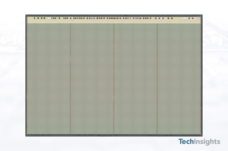
This is the memory array portion:

ymtc-fig4.jpg


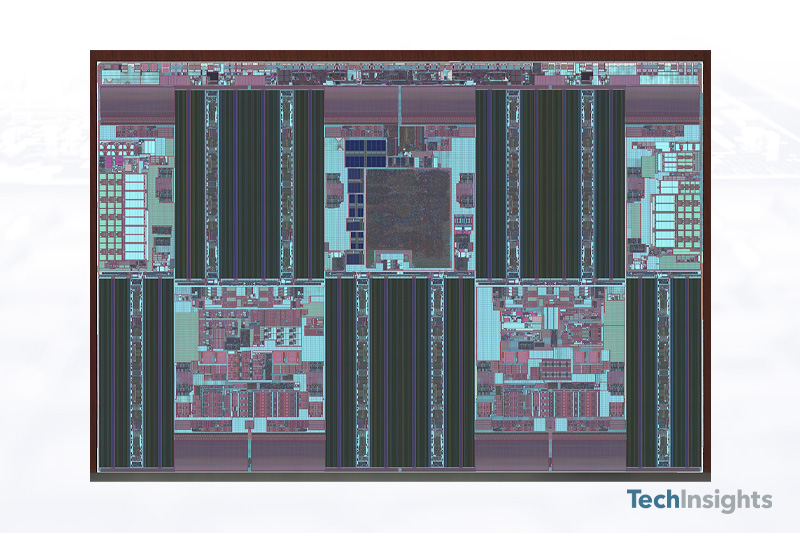
This is the logic circuit portion:

ymtc-fig5.jpg

It would not make sense to describe both using memory array naming rules, you can tell with your eyeballs that they're nowhere near the same process!

I've also only found literature stating 180 nm is the process used for the peripheral circuits.
Please, Log in or Register to view URLs content!


It's not unreasonable either. Intrachip data transfer can be blazingly fast.
Please, Log in or Register to view URLs content!
and
Please, Log in or Register to view URLs content!
Even Ethernet I/O which is long distance can reach GB/s regularly.
Please, Log in or Register to view URLs content!
.
 
Status
Not open for further replies.
Top