Is Newport really UK's leading fab? So UK is only at 180nm?The funny thing is this "leading edge" UK semi fab is worse than the Russian ones.
At least the Russians have 90nm. They are still stuck at 180nm.
And then they laugh about the Russian semi industry.
Which is pathetic but the great British empire is, as you see.
That they think the Chinese industry needs this acquisition for the "technology" is laughable.
It is just a nice deal for a cheap fab. It is cheaper to buy old facilities than make new ones.
But Wingtech is also building new ones. In China. Way better than this crap.
You are using an out of date browser. It may not display this or other websites correctly.
You should upgrade or use an alternative browser.
You should upgrade or use an alternative browser.
Chinese semiconductor industry
- Thread starter Hendrik_2000
- Start date
- Status
- Not open for further replies.
Yes. Pathetic no? The UK is one of those countries where the industry has gone into high end chip design and licensing of designs. ARM and Imagination Technologies for example. Even then while the chip design industry is there, and makes viable designs, ARM is currently owned by a Japanese company and Imagination Technologies by a Chinese one. They put it in the stock market. So guess what the companies with lots of capital own them. Their fabrication is near gone. The US was going the same route, until they decided it was dangerous and are now going to waste dozens of billions in fabs which I doubt will ever be fully utilized. Fabs which will likely cost twice the money to run and never run at 100% capacity. Should be an interesting money drain.
Last edited:
Wingtech buying this fab is probably the best way for the UK to save this fab. Will give a purpose to the fab and Wingtech will probably invest in new technologies for SiC and GaN.The funny thing is this "leading edge" UK semi fab is worse than the Russian ones.
At least the Russians have 90nm. They are still stuck at 180nm.
And then they laugh about the Russian semi industry.
Which is pathetic but the great British empire is, as you see.
That they think the Chinese industry needs this acquisition for the "technology" is laughable.
It is just a nice deal for a cheap fab. It is cheaper to buy old facilities than make new ones.
But Wingtech is also building new ones. In China. Way better than this crap.
If a Chinese company owns Imagine Technologies, does that mean China owns all the tech in that company?Yes. Pathetic no? The UK is one of those countries where the industry has gone into high end chip design and licensing of designs. ARM and Imagination Technologies for example. Even then while the chip design industry is there, and makes viable designs, ARM is currently owned by a Japanese company and Imagination Technologies by a Chinese one. They put it in the stock market. So guess what the companies with lots of capital own them. Their fabrication is near gone. The US was going the same route, until they decided it was dangerous and are now going to waste dozens of billions in fabs which I doubt will ever be fully utilized. Fabs which will likely cost twice the money to run and never run at 100% capacity. Should be an interesting money drain.
A couple of sentences form the article above to illustrate what is the US's idea of "ally". Please note that UK is not a random ally / partner country, actually it is US's right-hand man. UK is by far the closest and most supportive "ally" of US (although Australia is working hard to close the gap).
“The UK is a valued ally of the United States"
"If the UK does not stop the sale the congressmen are asking President Biden to reconsider Britain’s status on the “white list” of the US Committee on Foreign Investment."
"They have also asked President to to restrict exports of any US technologies or software used by Newport Wafer Fab"
@hvpc bro IF its okay for you to post my answer from your PM here, I been holding this Chinese Publication for 5 days now and perfect timing to answer part of your question.
This year, Apple glued two pieces of M1 Max together to make the M1 Ultra in seconds.
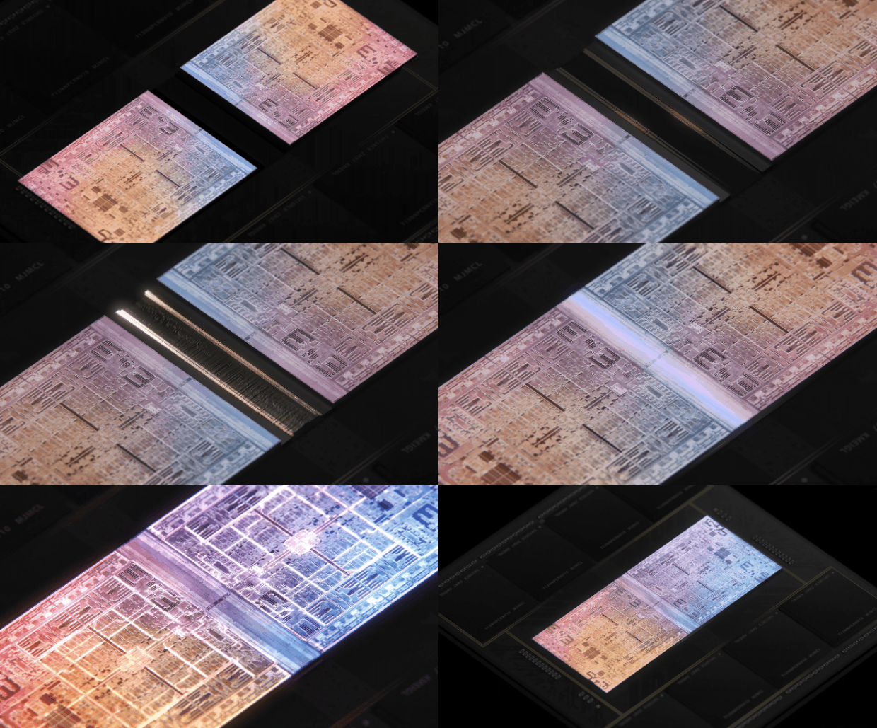
After sticking together , the performance has been greatly improved without changing the core process !

When talking about the chip technology process before, many machine friends will ask, when the chip technology reaches 1nm, how can the performance be improved?
Hey, it's not yet 1nm, can't you improve the performance without changing the process!

This time, it seems that Apple has suddenly found a fork in the road that can improve performance.
Recently, Huawei also published a patent for "sticky chips".
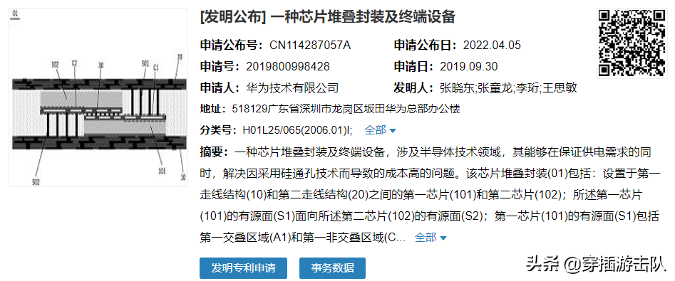
It seems that Apple's entry has made everyone stare at this plan at once.
Leading the industry again.
But ah, the truth is not all sauce purple.
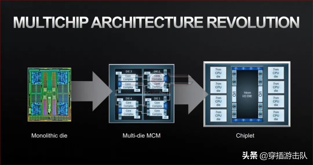
The technology of sticking chips used by Apple belongs to chiplet, also known as small chip technology.
At the beginning, when everyone had this idea, it was almost considered that the chip was made modular first.
The processing unit, storage, and I/O chips are separated, and these small chips are 3D packaged into a single chip through advanced packaging technology .
The combination of these three pieces forms the manufacturer's own solution.
Focus on two key points, split into small chips and advanced packaging technology .
This technology currently has at least three advantages.
One is that it can do super multi-core, and the performance will of course be stronger than a single chip. Needless to say about this M1 Ultra.
The second is that some solutions have a smaller area than directly installing two chips.
The third is to make good use of the cost, but it will reduce the cost.
The AMD team has given a case before. In the case of 14nm, the cost of separate production with small chip technology can be reduced by more than 40% compared to the direct integrated production of a single chip.
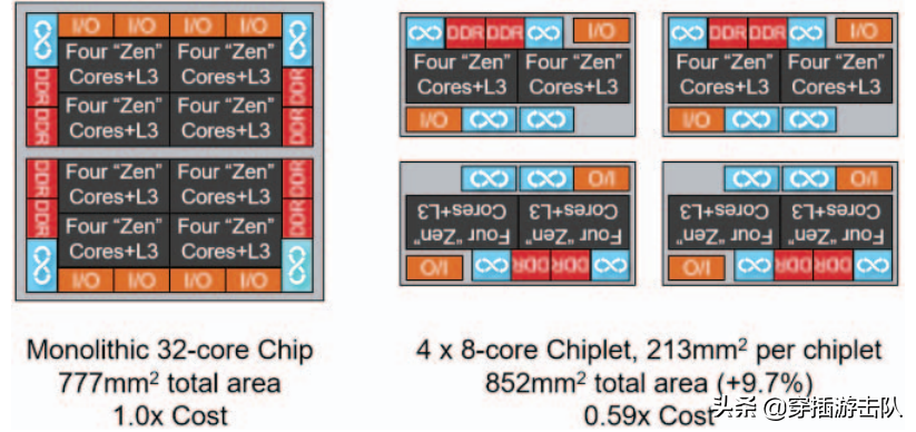
This small chip technology is also considered by some manufacturers as a solution to the failure of Moore's Law.
This technology, which can save money and improve performance when used well, doesn't have to wait for Apple at all .
Before M1 Ultra, AMD, Intel, Huawei, and Amazon all had related technical research on chiplet technology and mass-produced chips.
Such as AMD's ZEN/Ryzen, Intel's sapphire, Amazon's graviton.
In addition, the most powerful Huawei Kunpeng 920 in the industry is also made with this technology.
Huawei has made another major breakthrough, and Kirin chips are coming back?
2022-04-23 01:14 HKTThis year, Apple glued two pieces of M1 Max together to make the M1 Ultra in seconds.
After sticking together , the performance has been greatly improved without changing the core process !
When talking about the chip technology process before, many machine friends will ask, when the chip technology reaches 1nm, how can the performance be improved?
Hey, it's not yet 1nm, can't you improve the performance without changing the process!
This time, it seems that Apple has suddenly found a fork in the road that can improve performance.
Recently, Huawei also published a patent for "sticky chips".
It seems that Apple's entry has made everyone stare at this plan at once.
Leading the industry again.
But ah, the truth is not all sauce purple.
The technology of sticking chips used by Apple belongs to chiplet, also known as small chip technology.
At the beginning, when everyone had this idea, it was almost considered that the chip was made modular first.
The processing unit, storage, and I/O chips are separated, and these small chips are 3D packaged into a single chip through advanced packaging technology .
The combination of these three pieces forms the manufacturer's own solution.
Focus on two key points, split into small chips and advanced packaging technology .
This technology currently has at least three advantages.
One is that it can do super multi-core, and the performance will of course be stronger than a single chip. Needless to say about this M1 Ultra.
The second is that some solutions have a smaller area than directly installing two chips.
The third is to make good use of the cost, but it will reduce the cost.
The AMD team has given a case before. In the case of 14nm, the cost of separate production with small chip technology can be reduced by more than 40% compared to the direct integrated production of a single chip.
This small chip technology is also considered by some manufacturers as a solution to the failure of Moore's Law.
Simply put, it can meet the requirement of doubling the number of transistors and further improving the performance to a certain extent when the process is about to reach its peak.Moore's Law: The number of transistors that can be accommodated on an integrated circuit doubles about every two years and then extends to the chip cost. The cost can be reduced by 50% every one and a half years, and the average annual cost can be reduced by more than 30%.
This technology, which can save money and improve performance when used well, doesn't have to wait for Apple at all .
Before M1 Ultra, AMD, Intel, Huawei, and Amazon all had related technical research on chiplet technology and mass-produced chips.
Such as AMD's ZEN/Ryzen, Intel's sapphire, Amazon's graviton.
In addition, the most powerful Huawei Kunpeng 920 in the industry is also made with this technology.
continue....
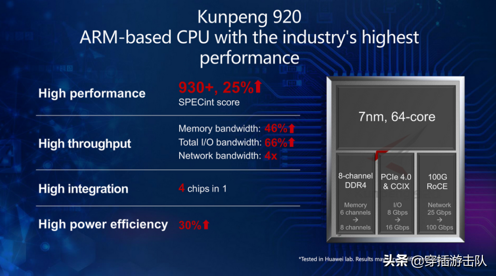
When it comes to Huawei, everyone will not be tired.
Huawei
Unlike several other manufacturers currently studying small chip technology, Huawei is limited in chips.
Several other companies may consider more ways to solve the two problems of expensive advanced processes and the failure of Moore's Law.
But for Huawei, in addition to the Kunpeng 920 server chip, it is also necessary to consider whether it can be easily alleviated, the problem that the mobile phone does not have its own chip.
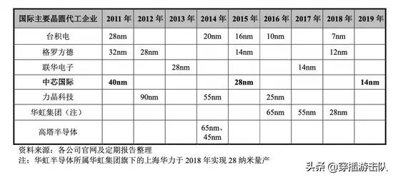
Before, Huawei asked SMIC to make a chip with a 14nm process, the Kirin 710A.
Its architecture is similar to that of the Kirin 970, both of which are 4×A73+4×A53, and the main frequency of the large core is 0.4GHz lower.
The main disadvantage is the GPU, only the quad-core Mali-G51.
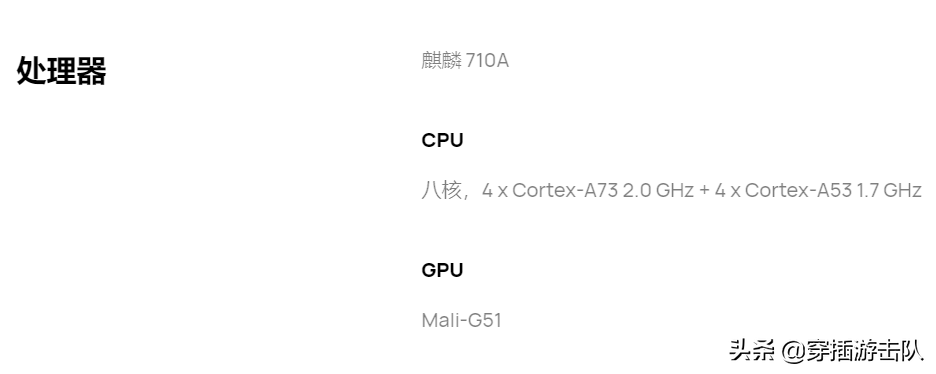
Due to various problems, the final AnTuTu score of this chip was only about 140,000 points .
Now, SMIC has upgraded to the FinFET N+1 process, which can achieve an effect close to 10nm.
There is also an N+2 process, which is expected to achieve performance close to 7nm.
However, in SMIC's 2021 financial report, there is no part of N+2 process research and development.
Therefore, its top-level process can only achieve performance close to 10nm.
Looking back, what are the characteristics of chiplet technology?
It is to increase the number of transistors and enhance performance through multi-chip stacking without improving the process.
Can Huawei use the chip stacking technology to stack 14nm or even close to 10nm chips to achieve stronger performance?

14nm+14nm=7nm is virtual, what about ≈7nm or >10nm?
Based on the information that Brother Ji has retrieved so far, it should be possible .
However, the problem is not small .
The key to small chip technology - advanced packaging, its top solution is still in the hands of TSMC.
In the case of Apple's M1 Ultra, the best thing about it is not stacking two chips together.
Instead - realize the interconnection bandwidth of up to 2.5TB/s between chips.
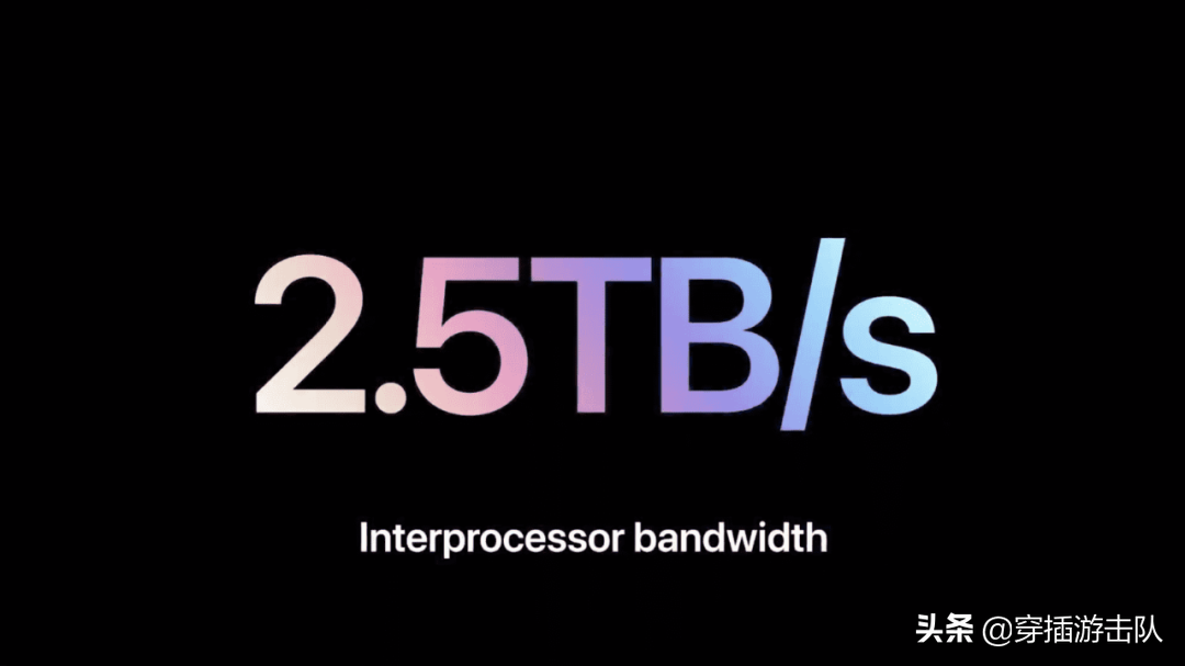
This is the fastest in the industry to do small chip technology.
When it comes to Huawei, everyone will not be tired.
Huawei
Unlike several other manufacturers currently studying small chip technology, Huawei is limited in chips.
Several other companies may consider more ways to solve the two problems of expensive advanced processes and the failure of Moore's Law.
But for Huawei, in addition to the Kunpeng 920 server chip, it is also necessary to consider whether it can be easily alleviated, the problem that the mobile phone does not have its own chip.
Before, Huawei asked SMIC to make a chip with a 14nm process, the Kirin 710A.
Its architecture is similar to that of the Kirin 970, both of which are 4×A73+4×A53, and the main frequency of the large core is 0.4GHz lower.
The main disadvantage is the GPU, only the quad-core Mali-G51.
Due to various problems, the final AnTuTu score of this chip was only about 140,000 points .
Now, SMIC has upgraded to the FinFET N+1 process, which can achieve an effect close to 10nm.
There is also an N+2 process, which is expected to achieve performance close to 7nm.
However, in SMIC's 2021 financial report, there is no part of N+2 process research and development.
Therefore, its top-level process can only achieve performance close to 10nm.
Looking back, what are the characteristics of chiplet technology?
It is to increase the number of transistors and enhance performance through multi-chip stacking without improving the process.
Can Huawei use the chip stacking technology to stack 14nm or even close to 10nm chips to achieve stronger performance?
14nm+14nm=7nm is virtual, what about ≈7nm or >10nm?
Based on the information that Brother Ji has retrieved so far, it should be possible .
However, the problem is not small .
The key to small chip technology - advanced packaging, its top solution is still in the hands of TSMC.
In the case of Apple's M1 Ultra, the best thing about it is not stacking two chips together.
Instead - realize the interconnection bandwidth of up to 2.5TB/s between chips.
This is the fastest in the industry to do small chip technology.
continue.....
Huawei Kunpeng is 400GB/s, AMD ZEN3 is 140GB/s.

With this ultra-high interconnection bandwidth , as the basis for the superposition of the performance of the two chips, it is one of the keys to the technology.
The packaging technology used by the M1 Ultra may be one of these two: CoWoS-L and InFO-L.
Both of these are TSMC's 3D packaging technology.
In addition to Apple, AMD also uses the TSMC solution.
As early as 2015, the Fury X graphics card was released with HBM technology, which is almost the first AMD to start small chip technology.
Most of the current 3D packaging technology also comes from TSMC.
Including the 3D V-Cache technology released last year, it is also based on TSMC's advanced packaging.

Like mastering advanced processes such as 7nm, 5nm, and 3nm, top-level advanced packaging technology is also in the hands of TSMC.
It is even said that it will be TSMC's specialty for a long time in the future.
At present, among the top manufacturers that can be named, only Intel and Samsung have a layout in advanced packaging.
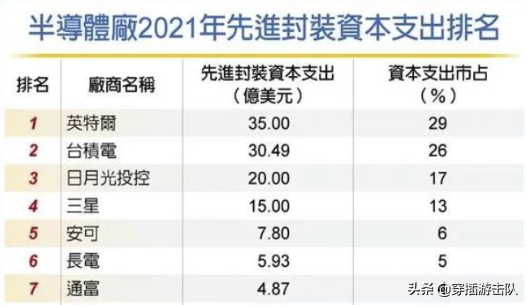
Intel's 2021 investment is huge.
However, many people predict that Intel is likely to turn back to a Fabless (fabless semiconductor) manufacturer that only designs chips and does not produce chips like AMD in the future.
As for Samsung?
Here are two excerpts from the reports:

Other packaging factories also have plans, but in the short term, advanced packaging will probably be dominated by TSMC and Intel.
What is the key to doing chiplet technology? It is the split and design of the core unit, as well as advanced packaging technology.
These packaging technologies are in the hands of Intel and TSMC... Then Huawei is still facing the current predicament.
You can do the chip design yourself, or you can do the chip stacking design yourself.
But the old question remains, who will produce?
Some machine friends may ask, what about SMIC?
SMIC can indeed produce 14nm chips, but he may not be able to handle advanced packaging.
This is a production problem.
There's also the problem of chiplet technology itself.
It is a technology that is more suitable for large chips. Whether it is cost considerations or the technology itself, it seems to be more suitable for large chips.
Let's deconstruct the cores of the two chips, stack them in one chip, let's not talk about whether the performance is ×2, the power consumption and heat generation must first be ×2.
It is not bad to be a processor for computers and servers. After all, active heat dissipation can be installed, and the power supply can also be charged up by several hundred watts.
Just imagine taking two Snapdragon 888s apart and sealing them like M1 Ultra, packaging them into such chips, and then stuffing them into the phone...
Not to mention the volume, this power consumption, this heat, can't you use water cooling?
Then there is the cost. At present, the mobile phone CPU may not be able to withstand the cost of advanced packaging + dual-chip stacking.
You have to understand that advanced packaging itself is more expensive than ordinary packaging .
Industry insiders have calculated that small chip technology can only benefit in two cases, one is to make larger chips, and the other is to make the most advanced advanced technology .
Part of the reason for a large chip is that the chip itself is very expensive. If it is produced in one piece, the cost of one component failure and the entire chip being scrapped is higher than the cost of advanced packaging.
The advanced technology machine brother understands that it is probably not able to make better chips, or when the next-level technology is used to make better chips, the price is more expensive.
At this time, advanced packaging can be used to obtain stronger performance.
But Huawei can only use SMIC's 14nm and N+1 solutions close to 10nm.
Stacking like this may become the price of a 5nm chip, making it close to the performance of a 7nm chip...
In this way, when facing 5nm competing products, there is neither performance advantage nor price advantage.
These two reasons also explain why both Samsung Electronics and Snapdragon are now looking down on advanced packaging.
Chiplets and advanced packaging are good things, and it is also a future trend, so Huawei is also doing it.
However, Huawei's current direction is to make chips for servers, not chips for mobile phones.
If you are interested, you can study the Kunpeng 920, which has very high performance.
As for the chiplet to make mobile phone chips, whether it can help Huawei mobile phones, we will wait and see.
Huawei Kunpeng is 400GB/s, AMD ZEN3 is 140GB/s.
With this ultra-high interconnection bandwidth , as the basis for the superposition of the performance of the two chips, it is one of the keys to the technology.
The packaging technology used by the M1 Ultra may be one of these two: CoWoS-L and InFO-L.
Both of these are TSMC's 3D packaging technology.
In addition to Apple, AMD also uses the TSMC solution.
As early as 2015, the Fury X graphics card was released with HBM technology, which is almost the first AMD to start small chip technology.
Most of the current 3D packaging technology also comes from TSMC.
Including the 3D V-Cache technology released last year, it is also based on TSMC's advanced packaging.
Like mastering advanced processes such as 7nm, 5nm, and 3nm, top-level advanced packaging technology is also in the hands of TSMC.
It is even said that it will be TSMC's specialty for a long time in the future.
At present, among the top manufacturers that can be named, only Intel and Samsung have a layout in advanced packaging.
Intel's 2021 investment is huge.
However, many people predict that Intel is likely to turn back to a Fabless (fabless semiconductor) manufacturer that only designs chips and does not produce chips like AMD in the future.
As for Samsung?
Here are two excerpts from the reports:
- In 2021, Samsung decided to deploy advanced packaging in order to compete with TSMC.
- In 2022, Samsung will reconsider whether advanced packaging needs a production line, because Qualcomm and Samsung themselves are currently not interested.
Other packaging factories also have plans, but in the short term, advanced packaging will probably be dominated by TSMC and Intel.
What is the key to doing chiplet technology? It is the split and design of the core unit, as well as advanced packaging technology.
These packaging technologies are in the hands of Intel and TSMC... Then Huawei is still facing the current predicament.
You can do the chip design yourself, or you can do the chip stacking design yourself.
But the old question remains, who will produce?
Some machine friends may ask, what about SMIC?
SMIC can indeed produce 14nm chips, but he may not be able to handle advanced packaging.
This is a production problem.
There's also the problem of chiplet technology itself.
It is a technology that is more suitable for large chips. Whether it is cost considerations or the technology itself, it seems to be more suitable for large chips.
Let's deconstruct the cores of the two chips, stack them in one chip, let's not talk about whether the performance is ×2, the power consumption and heat generation must first be ×2.
It is not bad to be a processor for computers and servers. After all, active heat dissipation can be installed, and the power supply can also be charged up by several hundred watts.
Just imagine taking two Snapdragon 888s apart and sealing them like M1 Ultra, packaging them into such chips, and then stuffing them into the phone...
Not to mention the volume, this power consumption, this heat, can't you use water cooling?
Then there is the cost. At present, the mobile phone CPU may not be able to withstand the cost of advanced packaging + dual-chip stacking.
You have to understand that advanced packaging itself is more expensive than ordinary packaging .
Industry insiders have calculated that small chip technology can only benefit in two cases, one is to make larger chips, and the other is to make the most advanced advanced technology .
Part of the reason for a large chip is that the chip itself is very expensive. If it is produced in one piece, the cost of one component failure and the entire chip being scrapped is higher than the cost of advanced packaging.
The advanced technology machine brother understands that it is probably not able to make better chips, or when the next-level technology is used to make better chips, the price is more expensive.
At this time, advanced packaging can be used to obtain stronger performance.
But Huawei can only use SMIC's 14nm and N+1 solutions close to 10nm.
Stacking like this may become the price of a 5nm chip, making it close to the performance of a 7nm chip...
In this way, when facing 5nm competing products, there is neither performance advantage nor price advantage.
These two reasons also explain why both Samsung Electronics and Snapdragon are now looking down on advanced packaging.
Chiplets and advanced packaging are good things, and it is also a future trend, so Huawei is also doing it.
However, Huawei's current direction is to make chips for servers, not chips for mobile phones.
If you are interested, you can study the Kunpeng 920, which has very high performance.
As for the chiplet to make mobile phone chips, whether it can help Huawei mobile phones, we will wait and see.
And to support the Chinese Publication authenticity , here is an article from Tom's Hardware as evidence written by Anton Shilov published yesterday. So the Chinese publication is not a fluke as it was fact checked by Western publication.
Huawei plans to boost performance for chips based on older nodes.
(Image credit: Panasonic)
Huawei has developed (and ) a chip stacking process that promises to be significantly less expensive than existing chip stacking methods. The tech will help Huawei continue to develop faster chips using older mature process tech, which could theoretically help it avoid US sanctions.
The only question is whether Huawei can actually take advantage of its innovation, given that foundries cannot produce chips for the company without an export license from the U.S. government. But at least Huawei itself certainly believes that it can, especially given that this tech could provide a performance boost for chips based on older nodes that aren't subject to such harsh US restrictions.
We'll get to the details of the new tech below, but it's important to understand why Huawei is developing this new tech. Since the U.S. government blacklisted Huawei and its chip design subsidiary HiSilicon and now requires all companies making silicon for them to apply for an export license since all semiconductor production involves technologies developed in the U.S., Huawei can't access any modern node (e.g., TSMC's N5), and therefore has to rely on mature process technologies.
To that end, innovative chip packaging and chiplet interconnection technologies in general as well as 3D stacking in particular is a way for the company to throw in more transistors into its SoCs and get the performance it needs to be competitive, said Guo Ping, Huawei's former rotating chairman, at a recent news conference, reports . Therefore, it makes great sense for the company to invest in proprietary packaging and interconnection methods, such as the one it patented.
"Micro-nano technology, exemplified by 3D hybrid bonding technology, will be the primary means to extend Moore's Law," said Guo.
The high-ranking executive from Huawei indicated that since modern leading-edge process technologies are progressing relatively slowly, multi-chiplet designs in 2.5D or 3D packages are a general way for chip designers to keep throwing more transistors into their products and meeting the expectations of their clients in terms of new features and performance. Therefore, Huawei will continue to invest in area enhancing and stacking technologies for in-house designs, the former chairman stressed.
The claim made publicly at a news conference clearly indicates that Huawei aims to use its hybrid TSV-free 3D stacking method (or maybe a similar and more mainstream method) for its upcoming products. The main question is whether the method requires any tools or technologies that the U.S. government may deem cutting-edge and not grant an export license (after all, most of the fab tools use technologies that originated in the USA). That said, whether we'll see a foundry making 3D chiplet packages for Huawei using the latter's patented method remains to be seen. But at least Huawei has a unique technology for inexpensive 3D stacking that can help it to stay competitive even without access to the latest nodes.
Innovative chip packaging and multi-chiplet interconnection technologies are set to become crucial in the next few years for leading-edge processors, and so all major chip developers and manufacturers now have their own proprietary chip packaging and interconnection methods.
Chipmakers generally use two packaging and interconnection methods: 2.5D packaging that enables a high-density/high-bandwidth in-package interconnect for chiplets sitting next to each other, and 3D packaging that makes processors smaller by stacking different chiplets on top of each other. However, 3D packaging typically requires rather complex wiring since chiplets need to communicate and power has to be delivered using TSVs.
While TSVs have been used in chip manufacturing for over a decade, they add complications and costs to the packaging process, so Huawei decided to invent an alternative solution without TSVs. What Huawei's specialists designed is essentially a hybrid between 2.5D and 3D stacking, as two chiplets overlap each other inside the package, saving space, but do not exactly sit on top of each other like in classic 3D packages.
Huawei's method uses overlapping parts of the chiplets to establish a logical interconnection. Meanwhile, two or more chiplets still have their own power delivery pins connected to their own redistribution layer (RDL) using a variety of methods. But while Huawei's patented technology avoids using TSVs, it does not look easy and cheap to implement.
Huawei's process involves flipping one of the chiplets upside down before connecting to another (or others). It also requires building at least two redistribution layers to deliver power (e.g., two chiplets means two RDLs, three chiplets can still use two RDLs, so do four, see the above gallery for details), which is not particularly cheap as it adds several additional process steps. The good news is that the redistribution layer of one of the chips can be used to connect things like memory, thus saving space.
In fact, Huawei's hybrid 3D stacking method may arguably be more universal than other companies' traditional 2.5D and 3D packaging technologies. For example, it is rather hard to stack two or three power-hungry and hot logic dies on top of each other, as cooling such a stack will be very complicated (which may ultimately mean compromises with clocks and performance). Huawei's method increases the surface size of the stack, which simplifies cooling. Meanwhile, the stack is still smaller than a 2.5D package, which is important for mobile applications like smartphones, notebooks, or tablets.
It is noteworthy that Semiconductor Manufacturing International Corp. (SMIC) with whom Huawei , is also betting on advanced packaging and interconnection technologies as on a way to get around sanctions imposed by the U.S. government. The company , so advanced packaging and interconnection methods are crucial for SMIC as well.
Other contract makers of semiconductors (TSMC, GlobalFoundries), integrated design manufacturers (Intel, Samsung), and even fabless chip developers (AMD) that can get access to leading-edge fab tools and process technologies also develop their own 2.5D and 3D chiplet stacking and interconnection methods to offer their clients or for their future products. Thus, Huawei is just following the curve.
1 day ago — Huawei is betting on advanced chip packaging to counter U.S. chip ... That said, whether we'll see a foundry making 3D chiplet packages for ...
Missing:14nm | Must include:
Huawei Turns To 3D Chip Stacking, Could Potentially Circumvent US Sanctions
By published 1 day agoHuawei plans to boost performance for chips based on older nodes.

(Image credit: Panasonic)
Huawei has developed (and ) a chip stacking process that promises to be significantly less expensive than existing chip stacking methods. The tech will help Huawei continue to develop faster chips using older mature process tech, which could theoretically help it avoid US sanctions.
The only question is whether Huawei can actually take advantage of its innovation, given that foundries cannot produce chips for the company without an export license from the U.S. government. But at least Huawei itself certainly believes that it can, especially given that this tech could provide a performance boost for chips based on older nodes that aren't subject to such harsh US restrictions.
A Way to Stay Competitive
We'll get to the details of the new tech below, but it's important to understand why Huawei is developing this new tech. Since the U.S. government blacklisted Huawei and its chip design subsidiary HiSilicon and now requires all companies making silicon for them to apply for an export license since all semiconductor production involves technologies developed in the U.S., Huawei can't access any modern node (e.g., TSMC's N5), and therefore has to rely on mature process technologies.
To that end, innovative chip packaging and chiplet interconnection technologies in general as well as 3D stacking in particular is a way for the company to throw in more transistors into its SoCs and get the performance it needs to be competitive, said Guo Ping, Huawei's former rotating chairman, at a recent news conference, reports . Therefore, it makes great sense for the company to invest in proprietary packaging and interconnection methods, such as the one it patented.
"Micro-nano technology, exemplified by 3D hybrid bonding technology, will be the primary means to extend Moore's Law," said Guo.
The high-ranking executive from Huawei indicated that since modern leading-edge process technologies are progressing relatively slowly, multi-chiplet designs in 2.5D or 3D packages are a general way for chip designers to keep throwing more transistors into their products and meeting the expectations of their clients in terms of new features and performance. Therefore, Huawei will continue to invest in area enhancing and stacking technologies for in-house designs, the former chairman stressed.
The claim made publicly at a news conference clearly indicates that Huawei aims to use its hybrid TSV-free 3D stacking method (or maybe a similar and more mainstream method) for its upcoming products. The main question is whether the method requires any tools or technologies that the U.S. government may deem cutting-edge and not grant an export license (after all, most of the fab tools use technologies that originated in the USA). That said, whether we'll see a foundry making 3D chiplet packages for Huawei using the latter's patented method remains to be seen. But at least Huawei has a unique technology for inexpensive 3D stacking that can help it to stay competitive even without access to the latest nodes.
Stacking Without Vias
Innovative chip packaging and multi-chiplet interconnection technologies are set to become crucial in the next few years for leading-edge processors, and so all major chip developers and manufacturers now have their own proprietary chip packaging and interconnection methods.
Chipmakers generally use two packaging and interconnection methods: 2.5D packaging that enables a high-density/high-bandwidth in-package interconnect for chiplets sitting next to each other, and 3D packaging that makes processors smaller by stacking different chiplets on top of each other. However, 3D packaging typically requires rather complex wiring since chiplets need to communicate and power has to be delivered using TSVs.
While TSVs have been used in chip manufacturing for over a decade, they add complications and costs to the packaging process, so Huawei decided to invent an alternative solution without TSVs. What Huawei's specialists designed is essentially a hybrid between 2.5D and 3D stacking, as two chiplets overlap each other inside the package, saving space, but do not exactly sit on top of each other like in classic 3D packages.
3D Stacking with Overlapping
Huawei's method uses overlapping parts of the chiplets to establish a logical interconnection. Meanwhile, two or more chiplets still have their own power delivery pins connected to their own redistribution layer (RDL) using a variety of methods. But while Huawei's patented technology avoids using TSVs, it does not look easy and cheap to implement.
Huawei's process involves flipping one of the chiplets upside down before connecting to another (or others). It also requires building at least two redistribution layers to deliver power (e.g., two chiplets means two RDLs, three chiplets can still use two RDLs, so do four, see the above gallery for details), which is not particularly cheap as it adds several additional process steps. The good news is that the redistribution layer of one of the chips can be used to connect things like memory, thus saving space.
In fact, Huawei's hybrid 3D stacking method may arguably be more universal than other companies' traditional 2.5D and 3D packaging technologies. For example, it is rather hard to stack two or three power-hungry and hot logic dies on top of each other, as cooling such a stack will be very complicated (which may ultimately mean compromises with clocks and performance). Huawei's method increases the surface size of the stack, which simplifies cooling. Meanwhile, the stack is still smaller than a 2.5D package, which is important for mobile applications like smartphones, notebooks, or tablets.
Not Alone
It is noteworthy that Semiconductor Manufacturing International Corp. (SMIC) with whom Huawei , is also betting on advanced packaging and interconnection technologies as on a way to get around sanctions imposed by the U.S. government. The company , so advanced packaging and interconnection methods are crucial for SMIC as well.
Other contract makers of semiconductors (TSMC, GlobalFoundries), integrated design manufacturers (Intel, Samsung), and even fabless chip developers (AMD) that can get access to leading-edge fab tools and process technologies also develop their own 2.5D and 3D chiplet stacking and interconnection methods to offer their clients or for their future products. Thus, Huawei is just following the curve.
1 day ago — Huawei is betting on advanced chip packaging to counter U.S. chip ... That said, whether we'll see a foundry making 3D chiplet packages for ...
Missing:
A flip chip type of interconnect is interesting. I don't know the details but I envision something like patterning an interchip communication only bond pad on the edge of a chip which attaches to another bond pad on the edge of another chip, then soldered together and packaged. The chips collectively talk to the outside world through other bond pads on one or both of the chips.And to support the Chinese Publication authenticity , here is an article from Tom's Hardware as evidence written by Anton Shilov published yesterday. So the Chinese publication is not a fluke as it was fact checked by Western publication.
Huawei Turns To 3D Chip Stacking, Could Potentially Circumvent US Sanctions
By published 1 day ago
Huawei plans to boost performance for chips based on older nodes.

(Image credit: Panasonic)
Huawei has developed (and ) a chip stacking process that promises to be significantly less expensive than existing chip stacking methods. The tech will help Huawei continue to develop faster chips using older mature process tech, which could theoretically help it avoid US sanctions.
The only question is whether Huawei can actually take advantage of its innovation, given that foundries cannot produce chips for the company without an export license from the U.S. government. But at least Huawei itself certainly believes that it can, especially given that this tech could provide a performance boost for chips based on older nodes that aren't subject to such harsh US restrictions.
A Way to Stay Competitive
We'll get to the details of the new tech below, but it's important to understand why Huawei is developing this new tech. Since the U.S. government blacklisted Huawei and its chip design subsidiary HiSilicon and now requires all companies making silicon for them to apply for an export license since all semiconductor production involves technologies developed in the U.S., Huawei can't access any modern node (e.g., TSMC's N5), and therefore has to rely on mature process technologies.
To that end, innovative chip packaging and chiplet interconnection technologies in general as well as 3D stacking in particular is a way for the company to throw in more transistors into its SoCs and get the performance it needs to be competitive, said Guo Ping, Huawei's former rotating chairman, at a recent news conference, reports . Therefore, it makes great sense for the company to invest in proprietary packaging and interconnection methods, such as the one it patented.
"Micro-nano technology, exemplified by 3D hybrid bonding technology, will be the primary means to extend Moore's Law," said Guo.
The high-ranking executive from Huawei indicated that since modern leading-edge process technologies are progressing relatively slowly, multi-chiplet designs in 2.5D or 3D packages are a general way for chip designers to keep throwing more transistors into their products and meeting the expectations of their clients in terms of new features and performance. Therefore, Huawei will continue to invest in area enhancing and stacking technologies for in-house designs, the former chairman stressed.
The claim made publicly at a news conference clearly indicates that Huawei aims to use its hybrid TSV-free 3D stacking method (or maybe a similar and more mainstream method) for its upcoming products. The main question is whether the method requires any tools or technologies that the U.S. government may deem cutting-edge and not grant an export license (after all, most of the fab tools use technologies that originated in the USA). That said, whether we'll see a foundry making 3D chiplet packages for Huawei using the latter's patented method remains to be seen. But at least Huawei has a unique technology for inexpensive 3D stacking that can help it to stay competitive even without access to the latest nodes.
Stacking Without Vias
Innovative chip packaging and multi-chiplet interconnection technologies are set to become crucial in the next few years for leading-edge processors, and so all major chip developers and manufacturers now have their own proprietary chip packaging and interconnection methods.
Chipmakers generally use two packaging and interconnection methods: 2.5D packaging that enables a high-density/high-bandwidth in-package interconnect for chiplets sitting next to each other, and 3D packaging that makes processors smaller by stacking different chiplets on top of each other. However, 3D packaging typically requires rather complex wiring since chiplets need to communicate and power has to be delivered using TSVs.
While TSVs have been used in chip manufacturing for over a decade, they add complications and costs to the packaging process, so Huawei decided to invent an alternative solution without TSVs. What Huawei's specialists designed is essentially a hybrid between 2.5D and 3D stacking, as two chiplets overlap each other inside the package, saving space, but do not exactly sit on top of each other like in classic 3D packages.
3D Stacking with Overlapping
Huawei's method uses overlapping parts of the chiplets to establish a logical interconnection. Meanwhile, two or more chiplets still have their own power delivery pins connected to their own redistribution layer (RDL) using a variety of methods. But while Huawei's patented technology avoids using TSVs, it does not look easy and cheap to implement.
Huawei's process involves flipping one of the chiplets upside down before connecting to another (or others). It also requires building at least two redistribution layers to deliver power (e.g., two chiplets means two RDLs, three chiplets can still use two RDLs, so do four, see the above gallery for details), which is not particularly cheap as it adds several additional process steps. The good news is that the redistribution layer of one of the chips can be used to connect things like memory, thus saving space.
In fact, Huawei's hybrid 3D stacking method may arguably be more universal than other companies' traditional 2.5D and 3D packaging technologies. For example, it is rather hard to stack two or three power-hungry and hot logic dies on top of each other, as cooling such a stack will be very complicated (which may ultimately mean compromises with clocks and performance). Huawei's method increases the surface size of the stack, which simplifies cooling. Meanwhile, the stack is still smaller than a 2.5D package, which is important for mobile applications like smartphones, notebooks, or tablets.
Not Alone
It is noteworthy that Semiconductor Manufacturing International Corp. (SMIC) with whom Huawei , is also betting on advanced packaging and interconnection technologies as on a way to get around sanctions imposed by the U.S. government. The company , so advanced packaging and interconnection methods are crucial for SMIC as well.
Other contract makers of semiconductors (TSMC, GlobalFoundries), integrated design manufacturers (Intel, Samsung), and even fabless chip developers (AMD) that can get access to leading-edge fab tools and process technologies also develop their own 2.5D and 3D chiplet stacking and interconnection methods to offer their clients or for their future products. Thus, Huawei is just following the curve.
1 day ago — Huawei is betting on advanced chip packaging to counter U.S. chip ... That said, whether we'll see a foundry making 3D chiplet packages for ...
Missing:14nm| Must include:
In my opinion the advantage over a TSV could be that you don't need an ultra high aspect ratio etch through the entire silicon wafer. In fact you only need to deposit additional surface pad space. This saves on equipment cost. In addition the area of a TSV is small, meaning you need highly precise XY alignment. You can make bond pads bigger and XY alignment is more forgiving.
The disadvantage is that you need a chip flip step and the package is still bigger than a fully stacked package with TSVs. That means more PCB space. Phones are PCB space limited but heavy equipment like routers and cell towers not so much.
- Status
- Not open for further replies.
