Chinese semiconductor industry

Status
Not open for further replies.

Strangelove

Colonel
Registered Member
Please, Log in or Register to view URLs content!

By Ma Si | chinadaily.com.cn | Updated: 2022-04-21 19:33

6261410da310fd2bec8491ed.png
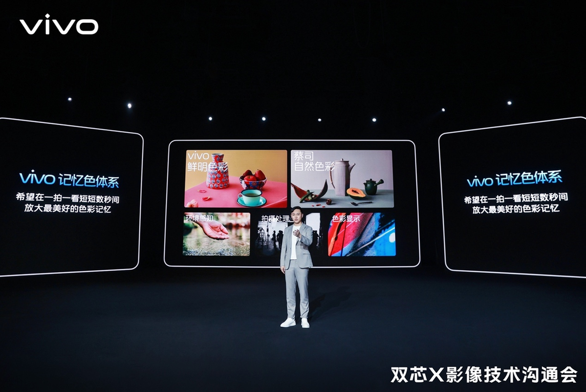
A Vivo employee shows how the company's latest chip helps improve mobile imaging. [Photo provided to chinadaily.com.cn]

Chinese smartphone vendor Vivo has unveiled its second self-designed chip as part of its broader push to beef up its research and development capabilities.

Known as V1+, the new chipset is designed to boost professional imaging and display performance of smartphones. The first model equipped with the new chip will be the X80 series, scheduled to be released next week.

Hu Baishan, executive vice president of Vivo, said as strategic technical partners Vivo and chipmaker MediaTek have brought in more than 300 researchers since last year to work on the collaborative development of the V1+ chip and the latter's Dimensity 900 processor.

More than 30 patents have been produced during the process, Hu said.

Vivo said the V1+ chip adapts 3D real-time stereo noise reduction, motion estimation and motion compensation technology in addition to featuring a high resolution ratio. Vivo also strengthens color management in four dimensions: detection, shooting, processing and display, to boost the mobile imaging experience.
 

hvpc

Junior Member
Registered Member
TMSC's Taiwan based fabs unable to supply the US and Chinese firms (remember, so many tech companies are on the entity list and more will be added in the coming months) and will not be viable. Hsinchu has a bleak future.
After the US sanction on Huawei, tsmc lost ~$1.8B of Huawei's business only to gain $2.1B from other US customers. And since stop selling to Huawei, tsmc had one record quarter after another. So I don't understand your view that Hsinchu's future is bleak.

Until anyone can catch up to tsmc's technology capability and capacity, their future is anything but bleak.
 

ansy1968

Brigadier
Registered Member
After the US sanction on Huawei, tsmc lost ~$1.8B of Huawei's business only to gain $2.1B from other US customers. And since stop selling to Huawei, tsmc had one record quarter after another. So I don't understand your view that Hsinchu's future is bleak.

Until anyone can catch up to tsmc's technology capability and capacity, their future is anything but bleak.
@hvpc bro in @Topazchen defense they created a competitor out of thin air whose potential may outlast them, TSMC may be the hero of today, BUT once Huawei and SMIC is able to mass produce a 7nm 3D chiplet in 2 to 3 years then let see, I for one think that TSMC had reach its zenith and from 2024 onward the Chinese FAB will eat a portion of their pie. And For god sake they just ban a country with a population of 145 million customer do you think the Chinese won't notice it, It's just a matter of time and lets see IF the Collective West can afford an Iphone powered TSMC chips. ;)
 

tokenanalyst

Brigadier
Registered Member
After the US sanction on Huawei, tsmc lost ~$1.8B of Huawei's business only to gain $2.1B from other US customers. And since stop selling to Huawei, tsmc had one record quarter after another. So I don't understand your view that Hsinchu's future is bleak.

Until anyone can catch up to tsmc's technology capability and capacity, their future is anything but bleak.
I thinks its referring to Hsinchu not just TSMC IF the U.S. mandate that semiconductors sold in the U.S are made domestically AND is also barred from making chips for China using U.S. equipment. That is an hypothetical scenario.

But I think an hypothetical scenario that could happen is that at other countries start increasing semiconductor manufacturing capacity with the excuse of "Because CHYNA" and "Muh National Security" the biggest loser could be the Taiwanese semiconductor industry if international clients decide to manufacture chips locally. The Taiwanese industry will be left with a diminishing pool of Chinese clients that will dry up with time as China semiconductor capabilities gets better.
 

tokenanalyst

Brigadier
Registered Member

ASML CEO: Industrial conglomerate buying washing machines to rip out semiconductors​

We've passed peak chip shortage, though, insists Gartner analyst​


A large industrial conglomerate is being forced to take increasingly desperate measures to satisfy their needs for chips, according to ASML, a manufacturer of chip-making equipment.
Talking on an
Please, Log in or Register to view URLs content!
this week with financial analysts, Peter Wennick, CEO at ASML, said that "width of demand" for chips was "significantly underestimated" by industry and: "I don't think that is going away."
"I met the executive of a very large industrial company, a conglomerate, last week, and actually they told me that they're buying washing machines to rip out the semiconductors to put them in industrial modules. I mean, that's happening these days," he said.

Please, Log in or Register to view URLs content!

Damn, talk about been desperation.
 

tokenanalyst

Brigadier
Registered Member
6-inch SiC high temperature epitaxy equipment was successfully developed in Jihua Laboratory

Recently, the SiC high-temperature epitaxy equipment independently developed by the high-power semiconductor research team of Jihua Laboratory has made a breakthrough. The team overcame the difficulties caused by foreign technology blockade and the epidemic. It took less than a year to complete the process from simulation simulation, structural design, temperature and gas field design, processing and procurement, to the independent development of system software, installation and debugging, and a A series of software and hardware joint debugging work has broken through a number of interdisciplinary problems, and has applied for more than 30 invention patents, of which 4 have been patented, and the main functions and performance indicators of the equipment have met the design requirements. At present, the researchers are conducting intense process debugging .
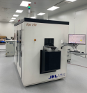


1650579928820.png
Epi 150 SiC epitaxy equipment physical photo

SiC epitaxy is the core process in the production process of SiC devices, and the production cost accounts for 22% of the device production process. Its production equipment is monopolized by developed countries such as Europe and the United States. The successful development of this equipment will solve the "stuck neck" problem that all the key process equipment used in the production of third-generation semiconductor SiC devices in my country relies on imports. The project adopts the design scheme of highly stable gas flow field, pressure field control, induction heating, and reaction chamber complete system, combined with self-developed in-situ monitoring technology, online cleaning technology and coating materials and processes, so as to realize the rapid and efficient SiC epitaxy. High-quality growth while improving the reliability and stability of equipment operation.

The core components of the equipment are all made in China, and the localization rate of the whole machine exceeds 85%. The equipment has achieved stable operation for nearly 30 hours for the first time. The background vacuum, leak rate, temperature control accuracy and other related indicators have reached the international advanced level, and some indicators such as the heating rate and the maximum process temperature are leading the international advanced level. The high-power semiconductor team also develops SiC epitaxy process and product development, SiC crystal growth process and equipment development, and SiC ion implantation process and equipment development. Based on scientific research, engineering and application are the goals to create a whole process chain covering core technologies. The R&D center leads the bright vision of the third-generation semiconductor equipment industry in the Guangdong-Hong Kong-Macao Greater Bay Area.
Please, Log in or Register to view URLs content!
 

tokenanalyst

Brigadier
Registered Member

ACM Research’s 18 Chamber, 300mm Ultra C VI Single-Wafer Cleaning Tool Enters Mass Production​


April 21, 2022 at 4:05 PM EDT

ACM’s Ultra C VI Tool Supports Most Semiconductor Clean Processes for Advanced Logic, DRAM and 3D NAND Manufacturing; Provides 50% More Throughput Than 12 Chamber Tool​

FREMONT, Calif., April 21, 2022 (GLOBE NEWSWIRE) --
Please, Log in or Register to view URLs content!
(ACM) (NASDAQ: ACMR), a leading supplier of wafer processing solutions for semiconductor and advanced wafer-level packaging (WLP) applications, today announced that its 18 chamber, 300mm Ultra C VI single wafer cleaning tool has been qualified by a customer and successfully moved to mass production. First introduced to the market in the second quarter of 2020, the tool has also been qualified for mass production by a mainstream memory chip manufacturer in China.​

“As technology nodes shrink, the complexity of chips is increasing, as are the number of wet cleaning process steps,” said Dr. David Wang, ACM’s President and Chief Executive Officer. “With the current unprecedented demand for semiconductor chips, the requirements for production capacity have become higher as well—and our 18 chamber system directly addresses this need. By moving our Ultra C VI tool to mass production, we can better serve our customers, allowing them to increase throughput by 50% versus the Ultra C V 12-chamber system, yet with a similar footprint.”​

About ACM’s 18 Chamber, 300mm Ultra C VI Tool
The 18 chamber, 300mm Ultra C VI tool is compatible with nearly all wet clean and wet etch processes. It can be used in several front-end and back-end applications, including polymer removal, tungsten (W) loop or back-end copper process, pre-deposition clean, post-etch and post-chemical mechanical polishing (CMP) clean, deep trench clean and RCA standard clean.​

The 18 chamber, 300mm Ultra C VI tool is equipped with one highly efficient wafer transfer system that consists of multiple robots, which allows the tool to reach a maximum throughput of more than 800 wafers per hour. The tool targets high-throughput cleaning, with a 50% increase in throughput, as compared to the Ultra C V 12-chamber system, due to the higher chamber count, with the same tool width and only a slight increase in length to allow for integration into existing production lines.

Please, Log in or Register to view URLs content!
 

gelgoog

Lieutenant General
Registered Member
The funny thing is this "leading edge" UK semi fab is worse than the Russian ones.
At least the Russians have 90nm. They are still stuck at 180nm.
And then they laugh about the Russian semi industry.
Which is pathetic but the great British empire is, as you see.

That they think the Chinese industry needs this acquisition for the "technology" is laughable.
It is just a nice deal for a cheap fab. It is cheaper to buy old facilities than make new ones.
But Wingtech is also building new ones. In China. Way better than this crap.
 
Status
Not open for further replies.
Top