No, about the so-called "thailand_guy".Are you talking about me, calling me sleepy loser?

You are using an out of date browser. It may not display this or other websites correctly.
You should upgrade or use an alternative browser.
You should upgrade or use an alternative browser.
Chinese semiconductor industry
- Thread starter Hendrik_2000
- Start date
- Status
- Not open for further replies.
[Patent decryption] SMIC invented the transmission gate crystal structure memory scheme
[Jiaqin Comments] The memory solution with the transmission gate crystal structure invented by SMIC can make the channel current of the transmission gate transistor smaller than the channel of the pull-down transistor by controlling the length of the channel region of the transmission gate transistor. Therefore, it is beneficial to increase the ratio of the memory, thereby improving the read tolerance of the memory.
As a typical semiconductor device, static random access memory (SRAM) has been widely used in electronic devices such as computers, mobile phones, and digital cameras.
With the development of semiconductor technology, the preparation process of memory has become more and more mature, and the formed memory also has better performance. In actual production scenarios, some manufacturers use fin-effect transistors as transistor devices in memory. Although the fin field effect transistor is applied to the memory, it is beneficial to reduce the size of the memory and also improve the performance of the memory. However, the performance of the memory needs to be further optimized, such as improving the read tolerance of the memory.
To this end, SMIC applied for an invention patent (application number: 201710322968.X) on May 9, 2017 called "memory and its formation method", the applicant is SMIC Integrated Circuit Manufacturing (Shanghai) Co., Ltd. company.
According to the relevant information currently disclosed in the patent, let us take a look at this solution.
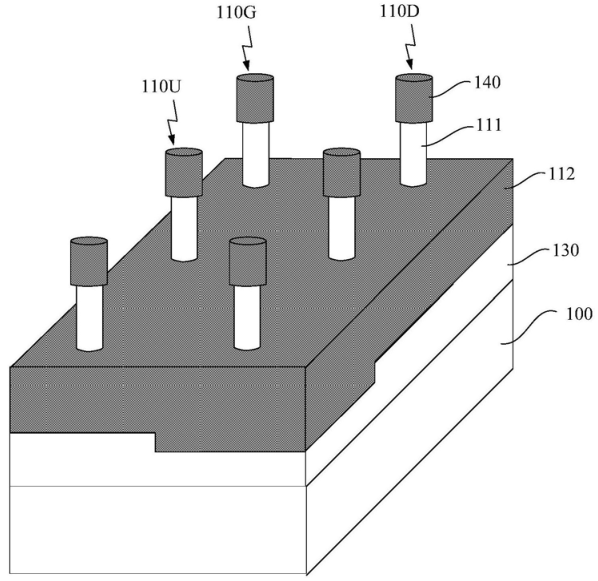
As shown in the figure above, it is a schematic diagram of the structure of the memory invented in this patent. The memory includes a substrate 100, a pull-down transistor (PD) 110D and a pass-gate transistor (PG) 110G, wherein the pull-down transistor and pass-gate transistor are both arranged on the substrate, and the lining The material of the bottom is usually in the form of silicon, germanium or a mixture of germanium and silicon, and the length L1 of the channel region of the pass-gate transistor is greater than the length L2 of the channel region of the pull-down transistor.
Also included on the memory is a pull-up transistor (PU) 110U, which is a transistor device with a wraparound gate, such as a wraparound gate nanowire field effect transistor (GAA NWFET). The pull-up transistor also includes nano-pillars 111 and gate structures 112, and the nano-pillars constitute the source and drain regions of the transistor.
oh good. I thought I said something wrong, again. haha.No, about the so-called "thailand_guy".
Satellite images matched with on the ground imagesLol what are your taking about? Satellite images of foundry? I sure there are lots of satellite images of large flat buildings in China.
So satellites can see through buildings now huhSatellite images matched with on the ground images
We had an offensive spammer called sleepy student a while ago. He got banned and returned with an alt account. As he get banned he kept coming back with alt accounts. If you go to the thread of banned users you can see the history of his alts getting banned. There is quite a lot. And every time he returned he was easily recognizable from his writing style. Deino can almost instantly recognize and ban him nowadays.Are you talking about me, calling me sleepy loser?
No, would expect satellites to spot corporate logos on the building and on packaged equipment materialsSo satellites can see through buildings now huh
Ok pay a satellite service to scan the movements of the thousands of Km^2 of industrial, technology parks and others locations in China almost daily, to find out a small fab that Huawei may have out there. If you can do that and post the results here the we can have a talk.Satellite images matched with on the ground images
@Michaelsinodef, there is a lot of effort needed to take a system good enough for 28nm production to enable 14nm/10nm/7nm.From what I understood from like reading this thread, the 28nm DUV by SMEE should also be able to make stuff like 14nm chips and possibly also 10nm (not sure about 7nm)
I mentioned this before, imaging resolution is all everyone ever talk about. Just because you could meet requirement for 28nm, one can't simply execute multiple patterning and expect to enable 14nm.
The overlay requirement for the most difficult step of 28nm node is 5nm-ish. SMIC's 14nm node overlay is like 3.5nm (that's a 30% improvement), and for 7nm node it's closer to 2~2.5nm. With multiple patterning, it's even more difficult than just 5nm to 3.5nm improvement...the extra patterning makes the need for more steps to match to one another steps is even more complex than simple 28nm technology.
28nm are typically made with ASML NXT1950i. SMIC uses NXT1980/NXT2000 for their 14nm. These are three and four generation more advanced systems than the 28nm system. In real life, it's not as easy as everyone seemed to make it out to be.
Since no one know what performance SMEE's immersion system is targeting. No one really knows for sure what this initial system could do. Everyone one on the web assumes 28nm. Because this is basically one of the last of the plane node. at 14nm below requires FINFET....so it's assumed 28nm would be a good target for SMEE to conquer first. But then, again, SMEE could be shooting for the moon/bet big on their first attempt.
But if 28nm is indeed SMEE's initial target, then to go to 14nm and below will require SMEE to put in even more effort.
Hope this explanation makes sense to you. If not, let me know, I can explain in more detail to you in private so I don't spam others.
Last edited:
Just saying I would have expected something to leak out by this pointOk pay a satellite service to scan the movements of the thousands of Km^2 of industrial, technology parks and others locations in China almost daily, to find out a small fab that Huawei may have out there. If you can do that and post the results here the we can have a talk.
- Status
- Not open for further replies.