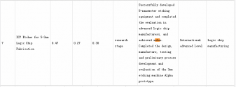
AMEC etchers have already been accepted for 5 nm process.I can’t say for sure because my experience is mostly with patterning and process control. But, I do believe it’s much easier to close the gap with the west in etching and deposition. So, I see indigenous etch, deposition, clean, & ion deposition, etc at a production ready level in a few years as highly feasible. If these companies are focused and continue to execute then I would go out on a limb and say they would be ready for 28nm by 2025. But that’s just my opinion. Maybe other expert in these areas could chime in and provide more solid assessment.
On your second question, I’m even less qualified to answer. But, smartphone is what’s driving the technology and the massive profit at tsmc. Chip performance, ultra low power consumption, small form factor are some key performance index that keep pushing tsmc to the brink of their capability. Without access to leading edge technology it’ll be hard for Huawei to come up with new/more powerful Kirin to compete with Apple.
BUT, Huawei has proven to be a world class tech conglomerate. I personally would not write them off just yet.
Finally people talk about etch and deposition lmao I was waiting for this.
The key challenge in etch is how to manage very aggressive chemistries such as fluorine and oxygen containing plasmas in a highly controlled way to achieve a huge variety of requirements (not all at once) including but not limited to:
1. Precision high aspect ratio etch for very deep, very narrow holes, for memory applications
2. High aspect ratio high speed etch for TSV, CMOS, packaging
3. Highly controlled large area etch for logic, perhaps even as precise as atomic layer etching
4.. Generally, high degrees of etch selectivity so only what you want to remove (oxides or nitride or resist) while avoiding what you don't want to remove (silicon or metal but also sometimes oxide/nitride)
5. Generally, etch uniformity across entire wafer or even multiple wafers which is a major challenge due to the relatively small dimensionality of plasma generators active region relative to the wafer size and high reactivity of the plasma.
6. Generally, extreme etch purity. Anything that reacts with wafer materials can also react with reactor chamber materials like aluminum and steel. These act as unintentional dopants if allowed to be exposed to the wafer. The exact coatings and materials used for the chambers to resist plasma and for plasma exposed components are highly advanced and much of the time, proprietary, in chemistry, fabrication and testing.
7. Inline process metrology for film thickness, wafer bow and plasma chemistry to adjust the reaction parameters (wafer chuck temperature and heating rate, plasma generation and chemical feed)
I can get into deposition but that's going to be some huge wall of text too.

