Hard to say, they initially wanted to mass-produce 3 nm in Q2 2022 but considering that there were news of problems in February, I think they will at least postpone to Q4 2022.@xypher bro question will they solve it before 2023?
You are using an out of date browser. It may not display this or other websites correctly.
You should upgrade or use an alternative browser.
You should upgrade or use an alternative browser.
Chinese semiconductor industry
- Thread starter Hendrik_2000
- Start date
- Status
- Not open for further replies.
coolieno99
Junior Member
The co-CEO of Synopsis is Chinese.For Companies that only had a few year in the market getting 5% of a competitive market like the GPU market is great start.
That is absolutely great, that means that means that in just 5 years Chinese SME manufacturers manage to catch 30% of the market and 50% of the component market.
"it will take xx years" means nothing, do you think in ten years all the sudden a EDA tool will appear from nothing?, I could mean that in just 5 years they could become as good synopsis and take at least 30% of the market share. Is a continuous development process that already started, that if favorable conditions like the U.S pressure continue it could push their industry even further.
Xiaomi Acquires Stake in Shanghai Chipmaker, Setting Ground for Car Ambitions
Shanghai AI Micron, an integrated circuit startup, recently added an industrial fund affiliate of tech giant Xiaomi to its list of shareholders, marking the latter’s new move to obtain the chipmaking technology key to its car-making endeavor.Meanwhile, the startup’s registered capital of the chipmaker increased from about CNY1.627 million (257,844) to about CNY1.8441 million, suggesting that the firm has recently raised funds from investors.
After the equity change, Hubei Xiaomi Changjiang Industrial Fund partnership (limited partnership) became the sixth-largest shareholder of AI Micron, owing 5.73% of the company.
The acquisition of a minority stake in the company aligns with Xiaomi’s plan to manufacturer intelligent electric cars (EV), a goal outlined in an official announcement as early as March 30, 2021. Lei Jun, founder and CEO of Xiaomi, served as the CEO of the new EV business.
Quickie
Colonel
Yes physical size has lost meaning in the semiconductor industry but in this case is the gate of the transistor is just like 3 atoms thick, probably deposit with atomic layer deposition method.
View attachment 85076
Looking at the diagram, the 3 atoms thick layer of the Gate has nothing to do with the process node size in the usual sense of those words.
For all we know, this work could have been done in a process node of 14 nm or even larger.
The paper refer to the size of the gate of the transistor, that is not done by lithography but by a fine atomic layer deposition technique. The rest of the transistor is probably done using lithographic techniques.Looking at the diagram, the 3 atoms thick layer of the Gate has nothing to do with the process node size in the usual sense of those words.
For all we know, this work could have been done in a process node of 14 nm or even larger.
Quickie
Colonel
The paper refer to the size of the gate of the transistor, that is not done by lithography but by a fine atomic layer deposition technique. The rest of the transistor is probably done using lithographic techniques.
Yes, that is what I have come to understand.
in general, after the 65 nm node or so, the "N nm" doesn't actually correspond to a physical dimension, it is more easily recognized as an "equivalent planar transistor density". Or to put it simpler - a brand name.That transistor is only 3 atoms thick . How can you go smaller that that.
For example TSMC 7 nm chips actually have transistor gate pitch of 54 nm:
What do you make of this paper?in general, after the 65 nm node or so, the "N nm" doesn't actually correspond to a physical dimension, it is more easily recognized as an "equivalent planar transistor density". Or to put it simpler - a brand name.
For example TSMC 7 nm chips actually have transistor gate pitch of 54 nm:
Chinese semiconductor industry
Non-American doesn't mean Chinese. It could also mean Dutch or Japanese and since litho (ASML) and the photoresist processing (Tokyo Electon) are not American but also not-Chinese, that 30% non-American is a much smaller Chinese proportion. Add two points to SME to 5% and that is global.
www.sinodefenceforum.com
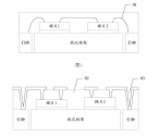
Huawei 3D stacking patent in 2021.


Abstract
The application discloses a chip packaging structure, a preparation method thereof and electronic equipment. The chip packaging structure includes: the semiconductor device comprises a first connecting layer, an upper surface bare chip, a first conducting structure, a first plastic packaging layer and a rewiring layer, wherein the first connecting layer is provided with an upper surface and a lower surface which are opposite, the upper surface bare chip is arranged on the first connecting layer, the first conducting structure is arranged on the upper surface of the bare chip, the first plastic packaging layer coats the bare chip and the first conducting structure, and the rewiring layer is arranged on the first plastic packaging layer;at least one part of the first conduction structure is exposed on the upper surface of the first plastic packaging layer, and the rewiring layer is coupled with the first conduction structure. The signals of the bare chips are directly led out through the first conducting structure and the rewiring layer, so that the space is saved, the wiring length and the interconnection inductance are reduced, and the low-loss and high-efficiency interconnection of the signals between the bare chips is realized; the signal interconnection between the bare chips is realized through the rewiring layer, and circuit wiring matched with the rewiring layer can be arranged in the rewiring layer according to the impedance value of the bare chips, so that components such as capacitors for coupling impedance are omitted, the space is saved,and the design complexity is reduced.What do you make of this paper?
It seems enormously significant to me as a layman, but I'd like to hear from someone with experience in the industry like yourself.Chinese semiconductor industry
Non-American doesn't mean Chinese. It could also mean Dutch or Japanese and since litho (ASML) and the photoresist processing (Tokyo Electon) are not American but also not-Chinese, that 30% non-American is a much smaller Chinese proportion. Add two points to SME to 5% and that is global.www.sinodefenceforum.com
Those are the expected results from a size perspective.
LW is the line width, which is in the tens of nm (22-68 nm)
LER is line error roughness. that's the deviation from straightness of a feature, not the feature size itself, and note how they're limited at around 2-3 nm. So errors get bigger relative to feature size as you move down in process.
What they're doing in that paper is developing an EUV photoresist with high resolution and testing a measurement platform. many photoresists in use now for ArF processes are polymeric resists which are easy to coat (spin coating the polymer solution) but have a resolution problem.
Let's take a positive photoresist - where exposed, it becomes more soluble. These contain a photoacid generator (PAG) which is an organic molecule that turns into a water soluble acid when exposed to UV light. This acid either directly dissolves away as part of the photoresist, or reacts with the photoresist.
Here's the problem - many organic molecules are soluble in polymers due to their loose pack molecular structure and similar chemical properties. So they'll move over time. Even motion of a few nm means that the edge of the exposed feature is no longer sharp. So for EUV, they need to develop a photoresist specifically for high resolution EUV processes.
- Status
- Not open for further replies.
