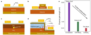
That transistor is only 3 atoms thick . How can you go smaller that that.I think we are approaching the economic limits of smaller transistors, even with EUV which is increasing the cost of semiconductors fabs by a lot, the cost of even designing the chips are in newer nodes is increasing exponentially.
I think that advanced packaging (geometrical scaling) could potentially become the cost effective alternative to get more computational power while keeping the cost down and that could be one of the three potential future problems for ASML who has made a lot of investment in EUV taking in consideration that will be widely adopted.
You are using an out of date browser. It may not display this or other websites correctly.
You should upgrade or use an alternative browser.
You should upgrade or use an alternative browser.
Chinese semiconductor industry
- Thread starter Hendrik_2000
- Start date
- Status
- Not open for further replies.
I don't think is possible because quantum mechanics and the randomness of nature start to become more relevant a those scales.That transistor is only 3 atoms thick . How can you go smaller that that.
3 nm is not the actual physical size.That transistor is only 3 atoms thick . How can you go smaller that that.
Looks like China is further ahead in SSMB Light Source research than we all think.Extreme Ultraviolet Photoresist Inspection Platform in Shanghai Synchrotron Radiation Facility
ZHAO Jun1,2, YANG Shu-Min2, XUE Chao-Fan2, WU Yan-Qing2*, CHEN Yi-Fang1, TAI Ren-Zhong2
Abstract: As the next generation of lithography technology, extreme ultraviolet lithography has been given the mission of saving Moore′s law by the industry. Extreme ultraviolet photoresist is one of the core sub-technologies of extreme ultraviolet lithography. The inspection of its resolution, roughness, sensitivity and outgassing conditions is a necessary condition for the development of extreme ultraviolet photoresist and it is also an important part to optimize the resist performance. Extreme ultraviolet interference lithography based on synchrotron radiation is currently the most suitable method for testing the performance of extreme ultraviolet photoresist. According to related research and development needs, an extreme ultraviolet photoresist inspection platform based on this method has been established in Shanghai Synchrotron Radiation Facility(SSRF). By continuously improving the stability of the device, developing independent beam splitting grating mask manufacturing technology, and constantly exploring and optimizing the corresponding interference exposure process, the current inspection resolution has reached below 20 nm, which basically meets the corresponding requirements for the 7 nm process node of extreme ultraviolet lithography.
View attachment 84976
View attachment 84977
ICRD and the Chinese Academy of Sciences have been working for quite a while on the SSMB Equipment at the Shanghai Synchrotron.
Looks like this Prototype SSMB Light Source Equipment is advanced enough to act as a Photoresist Inspection Platform.
China working on both SSMB EUVL and LPP EUVL at the same time.
@WTAN Sir from my previous post, the possibility that SMIC can mass produce 5nm and 3nm Chips IF they received SMEE EUVL LPP by 2023/24 or 2025 EUVL SSMB? with all the materials needed and research done and dusted?Looks like China is further ahead in SSMB Light Source research than we all think.
ICRD and the Chinese Academy of Sciences have been working for quite a while on the SSMB Equipment at the Shanghai Synchrotron.
Looks like this Prototype SSMB Light Source Equipment is advanced enough to act as a Photoresist Inspection Platform.
China working on both SSMB EUVL and LPP EUVL at the same time.
Last edited:
There's no indication that this is SSMB or that the SSRF can operate in a mode that allows SSMB formation. The synchrotron is being used as an EUV light source to do testing and verification on things like mirrors and photoresists. Any synchrotron can do that - they can generate smaller wavelength photons than EUV - but it's far too inefficient to be used as a light source for mass production of chips.Looks like China is further ahead in SSMB Light Source research than we all think.
ICRD and the Chinese Academy of Sciences have been working for quite a while on the SSMB Equipment at the Shanghai Synchrotron.
Looks like this Prototype SSMB Light Source Equipment is advanced enough to act as a Photoresist Inspection Platform.
China working on both SSMB EUVL and LPP EUVL at the same time.
This is very important work and it certainly pushes Chinese EUV lithography forward, but we have to be careful not to go farther than what the evidence we have supports.
Seems like advanced packaging and stacking will be the next big thing. As far as I know, both and are having HUGE problems with the yield rates for 3/4 nm processes, e.g. Samsung had a ~35% yield rate for Snapdragon 8 Gen 1 chip (4 nm) and even worse rates for their Exynos 2200.Yes physical size has lost meaning in the semiconductor industry but in this case is the gate of the transistor is just like 3 atoms thick, probably deposit with atomic layer deposition method.
View attachment 85076
@xypher bro question will they solve it before 2023?Seems like advanced packaging and stacking will be the next big thing. As far as I know, both and are having HUGE problems with the yield rates for 3/4 nm processes, e.g. Samsung had a ~35% yield rate for Snapdragon 8 Gen 1 chip (4 nm) and even worse rates for their Exynos 2200.
- Status
- Not open for further replies.

