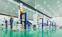
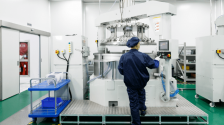
Cheer is the company who is making the Immersion systems for the SMEE DUVi machine.What is Cheer immersion system?
You are using an out of date browser. It may not display this or other websites correctly.
You should upgrade or use an alternative browser.
You should upgrade or use an alternative browser.
Chinese semiconductor industry
- Thread starter Hendrik_2000
- Start date
- Status
- Not open for further replies.
Yeah I agreeLet's talk about "concern" in the next decade. After all China's wake up moment just happened recently.
But the issue is that SMIC's progress is hamstrung without progress on the end of SMEE
Meanwhile TSMC has no such restrictions and continues to move ahead
The fear is the gap between TSMC and SMIC will not lessen, but widen moving forward.
SMEE just recently sent out 28nm machines for tested purpose, that's a good sign and I believe in the next 2 years the machine will be available for commercialisation. And I can see SMEE going to introduce a huge jump 14nm machine Or making a surprise of introducing the first indigenous develop EUV machine in 3/4 years time for a test purposeYeah I agree
But the issue is that SMIC's progress is hamstrung without progress on the end of SMEE
Meanwhile TSMC has no such restrictions and continues to move ahead
The fear is the gap between TSMC and SMIC will not lessen, but widen moving forward.
I think SMEE development path has been calculated. They know what's the goal to achieve. Developing a machine to manufacture the most Advanced node is one of their goal but the elephant in the room is older node that still in huge needs and highly used. Keep in mind that domestic fabrication market still mostly dominated by foreign SME suppliers so why jumping the focus on EUV when you still not develop highly competitive 28, 24, 14 nm DUV machines and not yer dominated your domestic market??
Honestly, people here don't pay that much attention on SMIC. Our biggest focus is on SMEE and other upstream suppliers.Yeah I agree
But the issue is that SMIC's progress is hamstrung without progress on the end of SMEE
Meanwhile TSMC has no such restrictions and continues to move ahead
The fear is the gap between TSMC and SMIC will not lessen, but widen moving forward.
The real gap is not between TSMC and SMIC, but between SMEE and ASML. And even here they are mostly system integrators, so we have to go even further upstream to make real comparisons
I have some questions for you knowledgeable guys. Do the latest high-end ASML DUV and Nikon DUV machines i.e 2050i and NSR-S635E have the ability to make high nanometer processes such as 65nm, 130nm etc or can they only be used for lower nanometer processes. If they can do 65nm etc are they good at that or would the process be worse than using an older machine whose maximum capability was 65nm? Also i have seen you guys say that nikon's machines are better than canon's machines but nikon is selling far fewer machines than canon. Is this due to price or are canon's machines better at some things, maybe image sensors or something? Do we know what lithography machines canon, nikon and sony use for the latest image sensors?
antiterror13
Brigadier
2050i can do 5nmI have some questions for you knowledgeable guys. Do the latest high-end ASML DUV and Nikon DUV machines i.e 2050i and NSR-S635E have the ability to make high nanometer processes such as 65nm, 130nm etc or can they only be used for lower nanometer processes. If they can do 65nm etc are they good at that or would the process be worse than using an older machine whose maximum capability was 65nm? Also i have seen you guys say that nikon's machines are better than canon's machines but nikon is selling far fewer machines than canon. Is this due to price or are canon's machines better at some things, maybe image sensors or something? Do we know what lithography machines canon, nikon and sony use for the latest image sensors?
i know, i'm wondering what the highest nanometer process it can do not the lowest.2050i can do 5nm
And yet TSMC is having yield problem with its 3nm while Samsung is having the same from its 10nm, 7nm and its much vaunted 5nm. Even without the necessary equipment, SMIC with its N+2 7nm is able to maintain a generation gap and from what I heard from hints from Chinese publication , SMIC have received ASML NXT 2050i able to produced 5nm chip using multi patterning and from Liang Mong Song, they had finished research on 5nm chips and even 3nm and just waiting for the necessary equipment, an excerpt below circa 2020.Yeah I agree
But the issue is that SMIC's progress is hamstrung without progress on the end of SMEE
Meanwhile TSMC has no such restrictions and continues to move ahead
The fear is the gap between TSMC and SMIC will not lessen, but widen moving forward.
I originally came to mainland China not to seek high-ranking officials, but simply to contribute to the mainland's high-end integrated circuits. At present, 28nm, 14nm, 12nm, and n+1 technologies have all entered mass production, and the development of 7nm technology has also been completed. Risk mass production will be available in April next year. The 8 most critical and most difficult technologies of 5nm and 3nm have also been carried out in an orderly manner [EMPHASIS ADDED]. Only when the EUV lithography machine arrives, we can enter the full development stage.
Note completed development of 7nm tech, SMIC had delivered better than Intel and with problems from TSMC 3nm and Samsung 5nm, I think by 2025 when China had introduced its EUVL powered by a SSBM, that gap will cease to exist.
7 days ago — According to a report quoting semiconductor industry sources, TSMC has trouble with its 3nm process yields. According to DigiTimes in Taiwan ...
7 days ago — The new report claims that the 4nm and 5nm yields were faked by Samsung Foundry executives to make it seem that everything was going well with ...
Missing:
Dec 17, 2020 — Mong-song Liang announced a surprise decision to resign from his role. Mr. Liang, who has been a key player in the Southeast Asian semiconductor ...
Last edited:
Hangzhou Semiconductor Wafer Co., Ltd., which was established in 2017 and is located in Dajiangdong Industrial Cluster, Qiantang New District, Hangzhou, is primarily engaged in the research, development and production of semiconductor wafers for high-quality integrated circuits.
In 2020, the Ferrotec Group made internal restructuring within the group, and finally achieved a vertical integration of its subsidiaries: Ferrotec (Ningxia) Semiconductor Co., Ltd. and Ferrotec Shanghai Semiconductor Wafer Co., Ltd. This allowed Ferrotec Hangzhou Semiconductor Wafer Co., Ltd. to perform the full integrated production from single crystal silicon ingots growing to wafer processing ranging from 100mm to 300 mm wafers for semiconductors. The plant currently has nine production lines for 8-inch wafers and two high-tech production lines for 12-inch wafers, with a total yearly production capacity of 2.4 million 300 mm wafers, 5.4 million 200 mm wafers and 4.8 million 150 mm wafers. FerroTec Hangzhou Semiconductor Wafer Co., Ltd strives to be one of the world's leading suppliers of semiconductor wafers, and realize the true nature of "smart manufacturing in China" in the semiconductor silicon material industry.


In 2020, the Ferrotec Group made internal restructuring within the group, and finally achieved a vertical integration of its subsidiaries: Ferrotec (Ningxia) Semiconductor Co., Ltd. and Ferrotec Shanghai Semiconductor Wafer Co., Ltd. This allowed Ferrotec Hangzhou Semiconductor Wafer Co., Ltd. to perform the full integrated production from single crystal silicon ingots growing to wafer processing ranging from 100mm to 300 mm wafers for semiconductors. The plant currently has nine production lines for 8-inch wafers and two high-tech production lines for 12-inch wafers, with a total yearly production capacity of 2.4 million 300 mm wafers, 5.4 million 200 mm wafers and 4.8 million 150 mm wafers. FerroTec Hangzhou Semiconductor Wafer Co., Ltd strives to be one of the world's leading suppliers of semiconductor wafers, and realize the true nature of "smart manufacturing in China" in the semiconductor silicon material industry.


- Status
- Not open for further replies.
