Chinese semiconductor industry

Status
Not open for further replies.

tokenanalyst

Brigadier
Registered Member
And yet TSMC is having yield problem with its 3nm while Samsung is having the same from its 10nm, 7nm and its much vaunted 5nm. Even without the necessary equipment, SMIC with its N+2 7nm is able to maintain a generation gap and from what I heard from hints from Chinese publication , SMIC have received ASML NXT 2050i able to produced 5nm chip using multi patterning and from Liang Mong Song, they had finished research on 5nm chips and even 3nm and just waiting for the necessary equipment, an excerpt below circa 2020.

I originally came to mainland China not to seek high-ranking officials, but simply to contribute to the mainland's high-end integrated circuits. At present, 28nm, 14nm, 12nm, and n+1 technologies have all entered mass production, and the development of 7nm technology has also been completed. Risk mass production will be available in April next year. The 8 most critical and most difficult technologies of 5nm and 3nm have also been carried out in an orderly manner [EMPHASIS ADDED]. Only when the EUV lithography machine arrives, we can enter the full development stage.

Note completed development of 7nm tech, SMIC had delivered better than Intel and with problems from TSMC 3nm and Samsung 5nm, I think by 2025 when China had introduced its EUVL powered by a SSBM, that gap will cease to exist.

Please, Log in or Register to view URLs content!

Please, Log in or Register to view URLs content!


7 days ago — According to a report quoting semiconductor industry sources, TSMC has trouble with its 3nm process yields. According to DigiTimes in Taiwan ...


Please, Log in or Register to view URLs content!

Please, Log in or Register to view URLs content!


7 days ago — The new report claims that the 4nm and 5nm yields were faked by Samsung Foundry executives to make it seem that everything was going well with ...
Missing: doctor ‎| Must include:
Please, Log in or Register to view URLs content!


Please, Log in or Register to view URLs content!

Please, Log in or Register to view URLs content!


Dec 17, 2020 — Mong-song Liang announced a surprise decision to resign from his role. Mr. Liang, who has been a key player in the Southeast Asian semiconductor ...
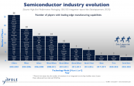
It is becoming exponentially difficult.
1646304486385.png
 

ansy1968

Brigadier
Registered Member
It is becoming exponentially difficult.
View attachment 84276
@tokenanalyst yup with SMIC and Huawei concentrating on 3D stacking chiplet, the most optimistic timeline IF TSMC is still having problem with its 3nm program, a parity performance wise by late 2023 IF both Huawei and SMIC are able to produce a 7nm 3D chiplet Vis a vis TSMC 5nm Chip.
 

tokenanalyst

Brigadier
Registered Member
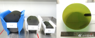
Recently, CETC Materials has successfully developed 8-inch silicon carbide crystals and realized the small batch production of 8-inch N-type silicon carbide polished substrates, further narrowing the technological gap at home and abroad, and providing independent guarantees for my country's silicon carbide business and laying a solid foundation for independent innovation and development.


1646309215700.png
 

spaceship9876

New Member
Registered Member
They can but typically for higher nm processes you can typically save cost with specialized wider projection area machines, or use 2nd hand refurbish machines. You only use brand new cutting edge machines for processes that you need them for.
If you wanted to make 5nm, 65nm and 130nm chips would it not be cheaper to buy the asml 2050i and use for all of these rather than buying 3 machines?
 

FairAndUnbiased

Brigadier
Registered Member
If you wanted to make 5nm, 65nm and 130nm chips would it not be cheaper to buy the asml 2050i and use for all of these rather than buying 3 machines?
no, absolutely not. the cost difference is gigantic. let's look at dry (1470k) vs immersion lithography (2050i).

Please, Log in or Register to view URLs content!
.

Within the DUV portfolio, the price differences are considerably larger. The most expensive DUV immersion systems use 193 nm light from an ArF laser and project their patterns through a water layer between lens and wafer. These cost around 60 million euros. The dry ArF systems fall into an entirely different price range, at around 20 million euros, while KrF machines cost 10 million euros.

Dry lithography is typically more productive as well. 1470k
Please, Log in or Register to view URLs content!
2050i produces
Please, Log in or Register to view URLs content!


This is easy to understand: the immersion system adds a new complication: the water handling.
Please, Log in or Register to view URLs content!
.

It requires expensive mechanisms to account for all these complications, you have to change to totally different photoresists, etc. It isn't easy and is very costly.

Dry lithography is far far far simpler than immersion because you don't have to worry about any of this which is reflected in the cost and the productivity.

Then you have older machines. This isn't a quote but typically you can get old dry ArF machines for ~5-10 million even with 100% brand new OEM parts. You can literally be producing profit on month 1 after install for a dry process while for immersion you're still not making money for years.
 
Status
Not open for further replies.
Top