a semiconductor device is nothing without several key added features.What special about this machine?
1. it has to be able to communicate with the physical world.
2. it has to be protected from the outside world while communicating with it
3. if not a complete SoC, it has to be able to interact with other chips for full functionality, with very low latency
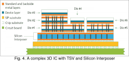
packaging deals with that. packaging is how you bring specialized chips together to form a full system within a single monolithic package. the black or metal looking flat chips with ball grid arrays on the bottom or pins on the edges that we see on PCBs? Those are not chips, those are packages with chips inside. Indeed, they may have multiple chips inside them simultaneously, all stacked to work together as a whole device.
How do you deal with the ultra thin connections between the chips that may have hundreds of data channels between them? how do you deal with defining the precise location inside the package where each chip sits? how do you deal with heat sinking for every chip? that's where packaging lithography comes in.

