Chinese semiconductor thread II

tokenanalyst

Lieutenant General
Registered Member

With a total investment of 4.5 billion yuan, the first 8-inch chip production line in Northwest China is empowering the leapfrog development of Shaanxi's semiconductor industry.​


Shaanxi TV reported on the construction of Northwest China's first 8-inch chip production line by Chip Industry Times. The production line is currently operating smoothly, with key process indicators and core equipment debugging fully meeting standards, injecting new momentum into Shaanxi's high-end semiconductor manufacturing.

Inside the modern, cleanroom of Chip Industry Era, an advanced 8-inch chip production line is operating at high speed. Since its trial production began last September, this production line, with a total investment of 4.5 billion yuan, has produced and sold thousands of wafers, with a product yield exceeding 95%. Reporters at the production site observed that all equipment in core process areas, such as lithography and etching, has been fully commissioned, and the cleanroom environment and plant power system have simultaneously met standards and been put into operation. This production line, designed to have a monthly capacity of 50,000 wafers, not only fills the gap in large-scale 8-inch chip manufacturing in Northwest China but also lays a solid foundation for the development of cutting-edge technologies such as silicon carbide.

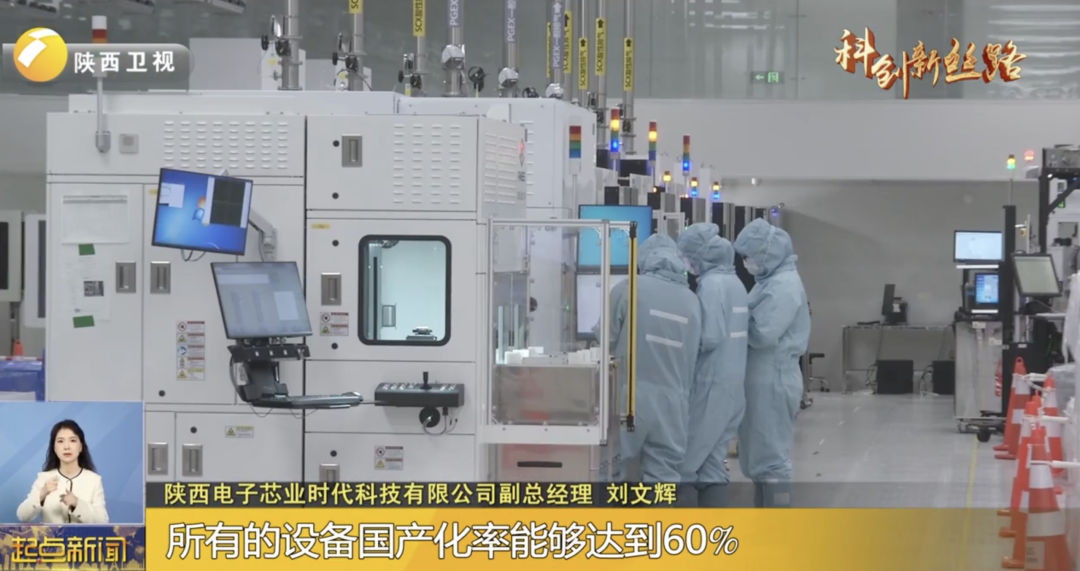
"From the very beginning of its construction, the chip manufacturing line was designed to be advanced from the outset. The localization rate of all equipment can reach 60%, and the localization rate of key components and raw materials can reach 90%. In particular, the entire production line uses brand-new equipment, and the level of automation of the entire equipment is the highest compared to other 8-inch lines in China. The whole line can achieve unmanned operation and unmanned factory," said Liu Wenhui, deputy general manager of Chip Industry Times.​
MBXY-CR-973851e1258edea0c7b5cccf6aae1d16.png

The 8-inch chip production line primarily targets industrial control fields such as electric drive control, charging conversion, and inverters for new energy vehicles. It is being built by Shaanxi Electronics & Information Group as the main investor, with the first phase having already completed an investment of 3.2 billion yuan. Currently, it has formed a complete "materials-design-manufacturing-packaging and testing" ecosystem with over 200 local semiconductor companies in Xi'an. Its entire production capacity for 2026 has already been booked, laying a solid foundation for future expansion.
Please, Log in or Register to view URLs content!
 

Michael90

Senior Member
Registered Member

Nexperia China is close to achieving 100% domestic semiconductor production.​


Nexperia's Chinese subsidiary is approaching a milestone of 100% domestic semiconductor production, aiming to fully localize its chip manufacturing by the second half of 2026. This strategic shift comes as a direct response to supply chain disruptions triggered by a geopolitical standoff between Nexperia's Dutch headquarters and its China-controlled parent company. Since last October, when Chinese export controls were imposed and wafer supplies from Europe were cut off, Nexperia China has been forced to pivot entirely toward using locally produced silicon wafers to maintain operations.

To circumvent these restrictions, Nexperia China has already begun manufacturing various chips using domestically sourced 12-inch wafers in its Dongguan packaging plant and Shanghai wafer facility, a move that contrasts with the Dutch parent's reliance on less advanced German 8-inch wafers. At a recent event in Beijing, company representatives confirmed they have transitioned from global to local supply chains, assuring customers that locally made chips will meet stringent quality standards. Despite this progress, current capacity remains around 60% to 70%, with plans to restore output to 90% by the second quarter of this year through a combination of inventory management and alternative domestic suppliers.

The conflict between the two entities stems from last September when the Dutch government invoked Cold War-era laws regarding state-owned enterprises, leading to administrative overreach that disrupted Nexperia China's access to office systems and internal communications. While the Dutch headquarters has historically sought dialogue to restore normal supply flows, these attempts have reportedly failed due to a lack of constructive engagement with Chinese management. As the situation evolves, Nexperia China is solidifying its Dongguan and Shanghai factories as primary production bases, ensuring that critical automotive, industrial, and consumer electronics components remain available within China despite the ongoing international friction.

Please, Log in or Register to view URLs content!
Ironically, this is actually a good thing for Chinese semiconductor suppliers. Own goal by the Dutch .
 

tokenanalyst

Lieutenant General
Registered Member

The "General Technical Specification for Laser Lifting and Thinning Equipment for Silicon Carbide Ingots," proposed by the Second Research Institute of China Electronics Technology Group Corporation (CETC), has been approved.​


On April 3, 2026, the Management Committee of the Alliance for Standardization of Third Generation Semiconductor Industry Technology Innovation Strategic Alliance (CASAS) officially approved the group standard proposal "General Technical Specification for Laser Lifting and Thinning Equipment for Silicon Carbide Ingots," submitted by the Second Research Institute of China Electronics Technology Group Corporation (CETC) and Beijing CETC Electronic Equipment Co., Ltd. This approval marks a significant step toward standardizing technical terminology and performance evaluation methods within the silicon carbide equipment industry. The Secretariat will now solicit drafting units from CASAS full members to form a standard drafting group, with further notices to be distributed via email.

The standard, designated T/CASAS 073, establishes comprehensive specifications for laser-based equipment used to slice silicon carbide (SiC) ingots. It covers definitions of specialized terms, equipment composition and functions, working conditions, technical requirements, testing methods, inspection rules, and guidelines for marking, packaging, transportation, and storage. Specifically, the document applies to equipment that uses a laser-modified system to non-contactly induce internal cracks within SiC ingots, separates wafers via a peeling and slicing system, and completes surface grinding through a thinning system. This technology supports processing of conductive, semi-insulating, and optical-grade SiC single crystals, addressing critical industry needs for consistency and quality control.

The development of this standard leverages the advanced capabilities of its proposing organizations. The Second Research Institute of CETC, China's only comprehensive electronics process research institute, contributes expertise in semiconductor materials, micro-assembly equipment, and intelligent manufacturing, with its laser stripping technology featuring multi-dimensional beam shaping and real-time focus correction for efficient 4–12 inch ingot processing. Beijing CETC Electronic Equipment Co., Ltd. complements this with its innovative silicon carbide thinning machine, which employs an automated dual-mode conveying system and independently developed ultra-precision air spindle technology to maintain wafer thickness deviation within 1 micrometer—achieving international advanced performance levels and supporting large-scale, high-yield SiC wafer production for next-generation semiconductor applications.

Please, Log in or Register to view URLs content!
 

tokenanalyst

Lieutenant General
Registered Member

Zowin Microelectronics Unveils Dual-Platform Strategy at 20th Anniversary​

Zowin Microelectronics (300782.SZ) celebrated its 20th anniversary in Wuxi by launching two strategic platforms: the MaxRF™ Superior RF Full-Stack Platform and the MaxExplore Lake Light Source Process Platform. Both platforms center on independent innovation and aim to reshape the boundaries of RF front-end and advanced semiconductor process technologies, providing strong momentum for industrial upgrades in the AI and IoT era.

Zowin Microelectronics began its RF technology journey in 2012 with a single GPS amplifier. Over the past two decades, the company has continuously expanded its product portfolio, building a complete matrix that includes RF switches, LNA banks, receiver modules, SAW filter modules, and high-end integrated modules. It has further extended into wireless connectivity fields such as WiFi, achieving a leap from single components to system-level solutions. By 2025, several of Zowin's L-PAMiD products achieved large-scale mass production and customer shipment, marking a significant advancement in RF front-end technology capabilities.

Liu Wenyong, VP of R&D at Zowin Microelectronics, explained that the MaxRF™ platform was built without shortcuts, adhering to self-reliance across device development, manufacturing processes, and R&D design. Through partnerships with Chiptronics and others, Zowin has established a complete resource loop covering specialized processes such as RFSOI, filters, gallium arsenide, IPD, and advanced packaging. He emphasized that with the approaching 6G era, AI technology will be leveraged to enable intelligent scenarios and reshape the RF front end, with continued innovation focused on higher-performance, more integrated, and smarter products.

The General Manager of Chipwise Lake Optics, noted that the subsidiary originated from supporting Zowin's RF business and has built solid industrial foundations in core RF processes like RFSOI and high-end filters. However, its exploration extends far beyond RF. He outlined Chipwise Lake Optics' strategic expansion into high-speed connectivity, energy management, low-power intelligence, optical communication, and MEMS—demonstrating a clear path from RF specialization to diversified technology leadership.

The launch of these two platforms represents a pivotal upgrade in Zowin's strategic positioning. The MaxRF™ platform marks a key step in strengthening its RF front-end leadership, while the MaxExplore Lake Light Source Process Platform signals the company's transformation from an "RF expert" to a "platform-based technology company." Both initiatives reflect Zowin's commitment to independent innovation, full-process control, and ecosystem collaboration.

Zowin Microelectronics views its 20th anniversary as both a milestone and a new starting point. Having completed the leap from "single-point breakthrough" to "platform construction" over two decades, the company is now positioned to address broader market opportunities. Driven by independent innovation and strengthened partnerships, Zowin aims to write another chapter of growth in the era of the Internet of Everything, unlocking new possibilities in connectivity, intelligence, and advanced semiconductor technologies.​

Please, Log in or Register to view URLs content!
 

Attachments

  • 1775532598688.png
    1775532598688.png
    124 KB · Views: 17

gotodistance

Junior Member
Registered Member
1. CXMT (DRAM 및 HBM)
• 2024: ~100,000 WPM level
• 2025: ~200,000 WPM
• 2026: ~300,000 WPM target = Top 3 global rankings
• 2027: 350,000-400,000 WPM
A structure that quickly approaches the level of Samsung (500,000) and Hynix (400,000)
CXMT aims to improve constitution and economies of scale at the same time, with high value-added lines centered on DDR5 and HBM (High Bandwidth Memory) rather than traditional DDR4.
• Shanghai New Fab Construction: It is building a production facility in Shanghai that is two to three times larger than Hefei's headquarters, with the goal of operating it in 2027. Equipment imports will begin in the second half of 2026.
· Target to Expand Production Capacity: We have already expanded our DRAM production capacity from 105,000 units per month at the end of 2023 to 250,000 to 270,000 units per month. With the expansion of the Shanghai plant, our production capacity is expected to double or triple its current capacity.
• Securing HBM Exclusive Line: By 2026, we plan to allocate approximately **20%** of total production capacity to mass production of HBM3 modules. Target wafer input is known to be around 60,000 units per month.
• Hefei Phase 2 Expansion: It will secure 40,000 additional production capacity per month through the Phase 2 expansion of its existing Hefei plant, bringing its total production to over 300,000 units per month.
• Technology Node: To avoid regulation, we are continuing to introduce equipment, naming the 17nm process 18.5nm class, and we are rapidly transitioning our lines to high-performance products such as DDR5-8000 and LPDDR5X.

2. YMTC (NAND Flash)
• 2023: 230,000 WPM level
• 2025: Over 400,000
• 2026: Projections for production of 500,000 WPM-class bits
• 2027: 550,000 to 600,000 WPM (2nd largest production scale)
Approaches similar levels to SK Hynix/Micron
YMTC is taking advantage of the lack of supply in the NAND flash market to accelerate the construction of "Wuhan Fab 3."
• Accelerating the Operation of Wuhan Plant 3 (Fab 3): We moved up the time of operation to the second half of 2026, which was originally targeted for 2027. The initial production capacity is 30,000 units per month, and it will be expanded gradually.
• Production Capacity Target: The operation of the third plant following the existing first plant (100,000 units per month) and the second plant (100,000 units per month) will greatly improve the overall production capacity. Through this, YMTC aims to achieve a 16% global NAND market share.
• High-rise NAND mass production: Using its own technology called 'Xtacking', it is building a 3D NAND mass production line with more than 300 levels and focusing on narrowing the technology gap with Korean companies such as Samsung Electronics and SK Hynix to less than a year.
• Diversifying Business: Nand as well as securing lines to enter the DRAM and HBM markets, including completing the production of LPDDR5 samples, are also included in the long-term plan.
 

tphuang

General
Staff member
Super Moderator
VIP Professional
Registered Member
Please, Log in or Register to view URLs content!


Just a couple of days after JFS Lab came out with 9000V MOSFET, Shenzhen Pinghu Lab & Garden Semi have come out with 10000V+ photoconductive switch


Please, Log in or Register to view URLs content!

Please, Log in or Register to view URLs content!

Great Bay Area's data center computation clusters already has 220 EFLOPS of computation in total and connected together with 400G all optical web achieving 1-10 ms latency. It is now adding a new cluster by Alibaba Cloud and China Telecom for 10k+ Zhenwu AI chip. This cluster expects to grow to 100k+ range in the future.
 
Top