Chinese semiconductor thread II

tphuang

General
Staff member
Super Moderator
VIP Professional
Registered Member
Please, Log in or Register to view URLs content!

Article from MIR Databank on the current state of China's photoresist industry. I actually think it's missing some players here like Bokang and I think Nanda and RA Chem aren't the only 2 doing Arf photoresist right now.

Note the domestic industry and penetration rate slides are as of 2024.

You can see for Jingrui, it made breakthrough with Arfi and 14nm+below process. In 2026, it has goal of expanding production capacity to 5000t for KRF & 1000t for ARF
 
Last edited:

tokenanalyst

Lieutenant General
Registered Member

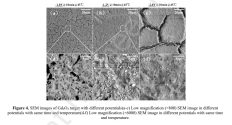
Spectral Characteristics of Gd2O3 Thin-Film Target for 6.7nm EUV Light Source.​

Abstract​

The extreme ultraviolet light source has been developed utilizing a Gd2O3 thin-film target, fabricated by the electrochemical deposition onto the ITO glass substrate. This study systematically investigates the influence of both electrochemical and laser parameters on the EUV radiation intensity of the Gd2O3 thin-film target. The experimental results indicate that strong extreme ultraviolet emission and a narrow spectral bandwidth were achieved with the specific deposition conditions. Comparative analysis reveals significant enhancements in the optimized thin-film target relative to a planar pure metal Gd target. Specifically, the width of the EUV spectrum from the thin-film target is narrowed to 3/5, the radiation intensity at 6.7 nm (within a 0.6% bandwidth) increases by a factor of 1.43, and the spectral purity improves by 32.3%. The work has demonstrated that employing the mass-limited Gd2O3 thin-film target can significantly improve EUV radiation characteristics. This approach holds promise for providing a novel concept in the development of next-generation EUV light source targets.

1768917958631.png
Please, Log in or Register to view URLs content!
 

ForcedTrend

New Member
Registered Member
TCL will be making all bravia TVs starting in april 2027

The new company plans to advance its business by leveraging Sony's high-quality picture and audio technology cultivated over the years, brand value and operational expertise including supply chain management, while utilizing TCL's advanced display technology, global scale advantages, industrial footprint, end-to-end cost efficiency, and vertical supply chain strength. The new company's products are expected to carry the globally recognized "Sony" name and "BRAVIA™" name, aiming to create new customer value through these branded products such as TVs and home audio equipment.

Please, Log in or Register to view URLs content!
 

tokenanalyst

Lieutenant General
Registered Member

Raysee Technology has completed a Series C financing round of hundreds of millions of yuan, which will be used for expanding the production capacity of VCSEL products, etc.​

Raysee Technology (Rayvision) has successfully closed a Series C financing round of hundreds of millions of yuan, led by a consortium of existing and new investors including Photon Strong Chain Fund, Hefei Industrial Investment, Shenzhen Capital Group, Xi’an Finance & Investment, Hony Capital, Open Source Innovation, and ABC Fund.

The funds will be primarily used to:​
  • Expand VCSEL chip production capacity
  • Accelerate R&D of core VCSEL technologies
  • Drive market expansion across key application sectors​
Founded in 2018, Raysee is a leading Chinese hard-tech semiconductor company specializing in VCSEL (Vertical Cavity Surface Emitting Laser) chips. It has achieved multiple industry firsts:​
  • First to mass-produce 2D addressable VCSELs for LiDAR
  • First to mass-produce short-wavelength red VCSELs
  • Pioneer of VIPE technology in consumer beauty devices​
  • First to apply VCSELs in robotic vacuum cleaners, capturing the #1 market share​
To date, Raysee has shipped over 200 million VCSEL chips, becoming the first domestic company to achieve 100% national production capability. Its 6-inch VCSEL wafer production exceeds 10,000 pieces annually, ranking #1 in China.

Its products are deployed in LiDAR, AI optical interconnects, smart cars, robotics, medical aesthetics, and industrial manufacturing, with annual revenue in the hundreds of millions of yuan, showing four consecutive years of rapid growth.

Raysee Technology is now positioned as a dominant domestic leader in VCSEL technology, driving innovation and supply chain independence in critical optoelectronic components.

Please, Log in or Register to view URLs content!
 

tokenanalyst

Lieutenant General
Registered Member

Suzhou releases action plan to promote high-quality development of the software industry, with EDA (Electronic Data Automation) highlighted.​


Suzhou has unveiled a comprehensive 2026–2027 Action Plan to accelerate the high-quality development of its software industry, with a strategic emphasis on Electronic Design Automation (EDA) as a critical national priority. The plan targets a ¥400 billion industry scale by 2027 and outlines six core domains: basic software, industrial software, application software, emerging platform software, information security software, and IT services. EDA, alongside CAD, CAE, and CAM, is singled out for focused investment in AI-enhanced design tools, 3D geometric modeling, and multiphysics simulation aiming to reduce China’s dependence on foreign semiconductor design tools and strengthen domestic supply chain resilience.

The plan sets ambitious targets for enterprise growth, innovation, and talent expansion: 600 municipal-level key software firms, 50 industry leaders, and 20 companies exceeding ¥1 billion in revenue; 2,000+ new software patents and 30,000+ copyrights; and a workforce of over 300,000, including 50 national-level experts.
To achieve this, Suzhou will build 16 specialized software industrial parks, with five targeting ¥10 billion in output, and establish regional clusters such as Xiangcheng for intelligent vehicles and digital finance, and the High-Tech Zone for IT innovation ensuring coordinated, differentiated development across the city.

Ten concrete actions underpin the strategy, including financial incentives for new software subsidiaries, up to ¥10 million in R&D grants for core tech breakthroughs, and ¥2 million rewards for new municipal parks. The plan promotes open-source ecosystems via the Open Atom Zijin Special Zone, encourages public-private scenario-driven innovation (e.g., manufacturing firms co-developing software), and supports talent attraction with up to ¥1 million in rewards for firms hiring top-tier experts. Additionally, Suzhou will launch 10+ service platforms for computing power, IP protection, testing, and standards, while promoting international standardization and patent development.

To ensure execution, the plan mandates strict oversight, inter-departmental coordination, and performance accountability, with implementation led by the Municipal Bureau of Industry and Information Technology. Policy alignment follows a “higher standard, no duplication” principle to avoid overlap. By integrating cutting-edge software innovation with industrial needs from semiconductors and smart manufacturing to digital finance and healthcare Suzhou aims not only to dominate China’s software landscape but to become a global benchmark for integrated, ecosystem-driven digital transformation, positioning EDA as a cornerstone of its technological sovereignty strategy.

Please, Log in or Register to view URLs content!
 

tokenanalyst

Lieutenant General
Registered Member

Tongfu Microelectronics' net profit is projected to reach 1.1 billion to 1.35 billion yuan in 2025, representing a year-on-year increase of 62.34% to 99.24%.​


On January 20, Tongfu Microelectronics released its 2025 annual performance forecast, expecting the net profit attributable to shareholders of the listed company to be between RMB 1.1 billion and RMB 1.35 billion, representing a year-on-year increase of 62.34% to 99.24%. The net profit after deducting non-recurring items also achieved a year-on-year increase of 23.98% to 56.18%, with basic earnings per share of RMB 0.72 to RMB 0.89.

In 2025, Tongfu Microelectronics will seize the structural growth opportunities in the global semiconductor industry, with mid-to-high-end products making a particularly significant contribution to revenue and becoming the core engine of performance growth.

At the same time, the company strengthened its operation and management and cost control, and made industrial investments around the upstream and downstream of the supply chain, which yielded substantial investment returns and further boosted its annual performance.

Please, Log in or Register to view URLs content!
 

tokenanalyst

Lieutenant General
Registered Member

A semiconductor front-end headquarters project with a total investment of 1 billion yuan was signed in Jiaxing.​

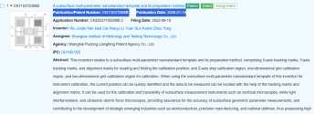
Jiaxing’s Nanhu District unveiled two major high-tech investments totaling 2 billion yuan, marking a significant leap in its ambition to become a hub for artificial intelligence and advanced manufacturing. The centerpiece of the ceremony was the semiconductor front-end equipment project, spearheaded by Suzhou Hangling Micro Precision Components Co., Ltd., a specialized innovator with 41 patented technologies. This 1-billion-yuan initiative will establish a “headquarters + manufacturing base” focused on producing critical components for wet and dry semiconductor processing equipment, directly supporting the local semiconductor supply chain and projected to generate 1 billion yuan in annual output upon full operation.
1768997911158.png


Complementing the semiconductor effort is the Embossed Mobile Robot Manufacturing Center, backed by Changsha Xingshen Intelligent Technology Co., Ltd. a leader in autonomous driving core technologies. Also investing 1 billion yuan, the company plans to leverage its expertise in AI-driven mobility to produce advanced embodied mobile robots. Once operational, this facility is expected to deliver an annual output value of 2 billion yuan, positioning Nanhu District at the forefront of China’s rapidly growing mobile robotics market. Company Chairman An Xiangjing emphasized the firm’s commitment to accelerating the commercialization of autonomous driving innovations, aiming to secure a leading global position in intelligent robotics.

Together, these two projects underscore Nanhu District’s strategic push to attract high-value, tech-intensive industries and diversify its industrial base beyond traditional manufacturing. By anchoring both semiconductor precision components and next-generation mobile robots under one regional ecosystem, Jiaxing is building a synergistic cluster that bridges advanced materials, automation, and AI key pillars of future industrial competitiveness. The investments not only promise substantial economic returns but also signal strong confidence from private sector leaders in the region’s innovation-friendly environment and policy support.

Please, Log in or Register to view URLs content!
 

tokenanalyst

Lieutenant General
Registered Member

JCET Group completes customer delivery of silicon photonics engine products, achieving a significant milestone in CPO technology.​


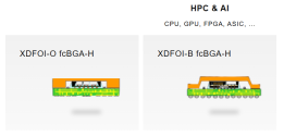
Shanghai, China, January 21 – JCET Group today announced significant progress in the field of co-packaged optoelectronics (CPO ) product technology. Its silicon photonics engine product , based on the XDFOI® multidimensional heterogeneous advanced packaging process platform, has completed customer sample delivery and successfully passed customer testing.

With the rapid growth of artificial intelligence and high-performance computing workloads, the demand for high-bandwidth, low-latency, and energy-efficient optical interconnect technologies continues to increase. CPO utilizes advanced packaging technology to achieve microsystem integration of optoelectronic devices and chips, providing a more compact and efficient implementation path for next-generation high-performance computing systems.

As a leading global provider of integrated circuit finished product manufacturing and technology services, JCET Group has actively expanded its presence in the CPO ( Consumer Product Provider) field, collaborating with numerous clients to offer comprehensive CPO solutions and supporting production capacity. JCET Group's optical engine product, utilizing the XDFOI® advanced packaging process, was recently successfully powered on at a client's site . This architecture achieves high -density integration of optoelectronic devices and logic chips within the package, effectively optimizing energy efficiency and bandwidth performance at the packaging level, thus supporting reduced system interconnect losses and improved overall scalability.
1768998408561.png

Silicon Photonics (CPO) plays a crucial role in both scale-up and scale- out networks and is considered the foundation of next-generation computing power. Meanwhile, with the continuous collaborative advancement of various segments of the silicon photonics industry chain, the CPO- related industrial ecosystem is gradually improving, covering key aspects from design and manufacturing to packaging, testing, and system verification.

Looking ahead, further breakthroughs and large-scale applications of CPO technology products will still depend on continuous collaborative innovation across all segments of the industry chain. JCET will continue to increase its investment in advanced packaging, focusing on building key capabilities such as multi-dimensional heterogeneous microsystem integration and optical testing, to provide advanced and reliable integrated circuit device manufacturing technologies and services for high-performance computing, data centers, and next-generation network systems.

Please, Log in or Register to view URLs content!
 
Top