Chinese semiconductor thread II

tokenanalyst

Lieutenant General
Registered Member

GaN Future's Gen3 Platform Launched.​


Zhuhai Gallium Future Technology Co., Ltd. has launched its Gen3 technology platform, featuring 650/700V series GaN field-effect transistors (FETs), marking a major advancement in power semiconductor performance.

Highlights:​
  • Innovative gate design delivers the strongest gate robustness among wide-bandgap devices, with simple gate driving compatible with traditional Si MOSFETs—enabling seamless integration into existing production lines.​
  • Achieves 25% lower reverse voltage drop than industry standards, improving system efficiency by 0.3–0.5 percentage points in high-frequency applications (e.g., EV inverters and DC/DC converters).​
  • Improved device performance: 33% reduction in die package width (DPW) and 15% optimization of FOM, enabling smaller footprint with enhanced power handling.​
  • Under high-load conditions (~7.7kW), temperature rise drops by 8.6°C (a 66% reduction) for the same Rds(on), boosting thermal stability and longevity.​
  • Offers nearly 20 package options, including TO-247, DFN, PQFN, TOLL, and QDPAK, supporting diverse applications from consumer electronics to industrial systems.​
GaN FETs are now embedded in mass-produced fast-charging adapters from leading global brands including Lenovo, DJI, Xiaomi, LG, HP, and Delta. These partnerships have enabled thinner, faster, and more efficient chargers delivering power delivery speeds up to 100W or higher while reducing heat generation and charging time for consumers.

GaN Future achieved a landmark milestone with the world’s first 3.6kW bidirectional energy storage inverter, enabling seamless energy flow between solar panels, batteries, and the grid. This technology is critical for smart homes and microgrids. Additionally, its 3kW communication power supply delivers up to 98% efficiency a significant improvement over conventional designs and supports stable operation under fluctuating loads, making it ideal for data centers and telecom infrastructure.

The company’s G3E65R009 series, the world's smallest 650V GaN discrete device with a record 1500A pulse current rating, represents a breakthrough in power density. This high-current capability enables more compact, efficient power conversion systems in electric vehicles (EVs), supporting higher output inverters and improved battery management. The device is currently undergoing R&D verification with several leading automotive OEMs and Tier 1 suppliers positioning GaN Future as a key enabler of next-generation EV drivetrains and on-board power electronics.

Expanding into High-Performance & Smart Systems: Beyond consumer and transportation, the Gen3 platform is being deployed in:

LED lighting (energy-efficient, high-lumen output with reduced driver losses),
High-performance computing (to manage power demands of AI accelerators and data centers),
Home appliances (e.g., smart fridges, air conditioners) for improved energy efficiency,
Motors & industrial drives, enabling faster response times and lower power consumption.​

Please, Log in or Register to view URLs content!
 

tokenanalyst

Lieutenant General
Registered Member

Jiangling Technology's AiMET AI Measurement System Empowers Semiconductor Measurement Performance​


Shanghai Jiangling Technology Co., Ltd. has successfully delivered a repurchased TFT70 SuperHiK high-end thin-film metrology system to a leading wafer fab in Shanghai marking a significant milestone as this is a repeat purchase, highlighting strong client confidence and sustained partnership.

TFT70 SuperHiK:
The flagship model in Jiangling’s TFT series, engineered with industry-leading SuperHiK® technology to deliver ultra-precise measurements for the most challenging thin-film layers in advanced semiconductor manufacturing:​
  • Gate ultra-high-k material (nano-thin single-layer films)
  • Metal interconnect layers (stacked nano-ultra-thin multilayer structures)
  • Ultra-thin dielectric layers
  • It has solved key international technical challenges and is already deployed in batches across logic and memory chip production lines, establishing a new supply security foundation for the front-end semiconductor industry.​
1763408037099.png
AiMET AI-Enhanced Metrology System (AI-powered):
A breakthrough integration of artificial intelligence into metrology, representing Jiangling’s deep application of AI in semiconductor process control. The AiMET system enhances every stage of data processing:​
  • Architecture: Uses a physically-supervised adaptive scaled neural network with high-reliability parallel computing for real-time, robust performance.​
  • AI Capabilities:
    • Data preprocessing, dimensionality reduction, classification, and prediction via machine learning.​
    • 20x faster analysis speed per wafer due to optimized AI inference algorithms.​
    • One-click recipe generation: Automatically designs customized measurement protocols for complex multi-layer films, boosting engineering efficiency and accuracy.​
    • Intelligent multi-layer model construction: Dynamically builds accurate models for diverse and intricate film stacks without manual intervention.​
    • Enhanced accuracy: AI-driven evolutionary algorithms significantly improve precision in measuring thin, complex films.​
    • Unified standards: Ensures consistent material coefficients and model building across different processes and sites, eliminating operational variability.​
The deployment of the AiMET system demonstrates Jiangling Technology's leadership in advancing intelligent metrology solutions. By combining cutting-edge hardware (TFT70 SuperHiK) with advanced AI software, the system delivers superior performance for high-end logic and memory chip manufacturing, directly supporting process control and yield optimization.

This success not only solidifies Jiangling’s position as a trusted supplier in the global semiconductor front-end ecosystem but also sets a new benchmark for intelligent, high-precision metrology systems.

Please, Log in or Register to view URLs content!
 

tokenanalyst

Lieutenant General
Registered Member

Small-area marks realize nanoscale lithography alignment by a spatial and frequency domain fusion neural network​


Abstract​


For traditional moiré-based lithography alignment technology, which is widely used in proximity lithography systems, complex alignment marks with larger areas are employed to achieve high-precision misalignment detection. However, every inch of space on the wafer is extremely precious in practice, leaving minimal space for alignment marks. Therefore, employing small-area alignment marks in lithography systems will be a very challenging task with considerable potential in the future. The primary challenge is that existing frequency-based analytical algorithms struggle to achieve misalignment values with high-precision from moiré fringe images generated by small-area marks. To address this challenge, a spatial and frequency information fusion neural network (SFFN) is proposed for processing the moiré fringe images. With SFFN, the area of the alignment mark can be reduced by 2/3, and the average error of SFFN is less than 1 nm on the test dataset.

Please, Log in or Register to view URLs content!
 

tokenanalyst

Lieutenant General
Registered Member
More information about this patent.

Innovative optical structure design
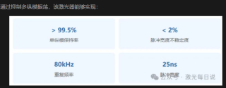
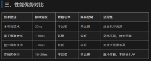
The laser employs a combined design integrating a quarter-wave plate, a Pockels cell, and a thin-film polarizer within the resonant cavity . Precise cavity emptying is achieved by electronically controlling the beam polarization state .
  1. First concave mirror the second concave mirror forms a resonant cavity with a radius of curvature of 658 mm.​
  2. CO₂ radio frequency waveguide placed inside the cavity, the waveguide aperture is 3mm, and the total length is 2.0m.​
  3. Quarter wave plate, the pockel cell and the gain medium are respectively placed at both ends.​
  4. Thin film polarizer as an output coupler​
Eliminate the spatial burning effect
In traditional cavity-blank lasers, the oscillating beam inside the radio frequency waveguide is linearly polarized, exhibiting a significant spatial hole-burning effect . This easily leads to multi-mode oscillations, resulting in multi-peak pulse waveforms.

This patent enables the beam of light propagating back and forth in the CO₂ radio frequency waveguide to form orthogonally circularly polarized light by precisely controlling the polarization state, and the light field is uniformly distributed in the light transmission direction, thus eliminating the spatial hole burning effect at the source.​

1763419943456.png
1763420112690.png

Please, Log in or Register to view URLs content!
 

tokenanalyst

Lieutenant General
Registered Member

Guangdong semiconductor "little giant" passed its IPO review! Backed by a major equipment manufacturer, it plans to raise 1.469 billion yuan.​

Just now, a Guangdong semiconductor "little giant" passed its IPO review! Backed by a major equipment manufacturer, it plans to raise 1.469 billion yuan.

Hengyunchang, a core component supplier of semiconductor equipment in Shenzhen, Guangdong, has just passed the review of the listing committee and taken another key step toward its IPO on the Science and Technology Innovation Board.

Founded in March 2013, Hengyunchang is a leading enterprise in the domestic plasma radio frequency power supply system industry and one of the very few domestic enterprises that have achieved mass production of semiconductor-grade plasma radio frequency power supply systems. It has been recognized as a key "Little Giant" enterprise of the National Specialized, Refined and Innovative Enterprises.

Plasma radio frequency power supply systems are one of the most difficult aspects of the localization of semiconductor equipment components. They are key to the process control of semiconductor manufacturing processes such as thin film deposition, etching, ion implantation, cleaning and resist removal, and bonding, and directly determine the equipment's process capability and product yield.
According to Frost & Sullivan, in 2024, the localization rate of plasma RF power supply systems in China's semiconductor industry was less than 12% , and Hengyunchang ranked first in market share among domestic plasma RF power supply system manufacturers .
Over the past decade, Hengyunchang has launched three generations of plasma RF power systems—CSL, Bestda, and Aspen—successfully breaking the decades-long monopoly held by the two major American giants, MKS and AE, in the domestic market. Its mass-produced products have reached the next-generation technological level of leading international companies, supporting 7-14nm processes.
1763420596090.png

In the domestic semiconductor field, Hengyunchang is the first domestic manufacturer to ship over 100 million yuan worth of products and the first to achieve mass production of plasma radio frequency power supply systems (supporting advanced semiconductor processes) .

Its product series has been continuously verified and delivered in batches by leading domestic semiconductor equipment manufacturers such as Topway Technology, AMEC, NAURA, and MicroNano , and is also used by domestic wafer fabs such as SMIC and Yangtze Memory .

Please, Log in or Register to view URLs content!
 
Top